History of Apple Computer Models
I have been an Apple programmer specializing in high-performance applications since the Apple II in 1980. My interest in processor performance is almost as old (see for example Super MANDELZOOM, my A005646 calculations, Sloandora and my Gray-Scott explorer). I continue to use my software from the 1980's and 1990's through emulators.
Details of Certain Specific Systems
Apple's Special Relationship With Intel
High-Level Design
Intel Product Cycle
Overview of Recent Intel Codenames
Chronology of Intel Silicon Fabrication Process Technology
Silicon Fabrication Advances
Intel's New Process Announcements
Chronology of Memory Products and Process Technology
Recent Memory Module Characteristics and Performance
PowerPC
Appendix B: Silicon Technology
Appendix D: The Detritus of Research
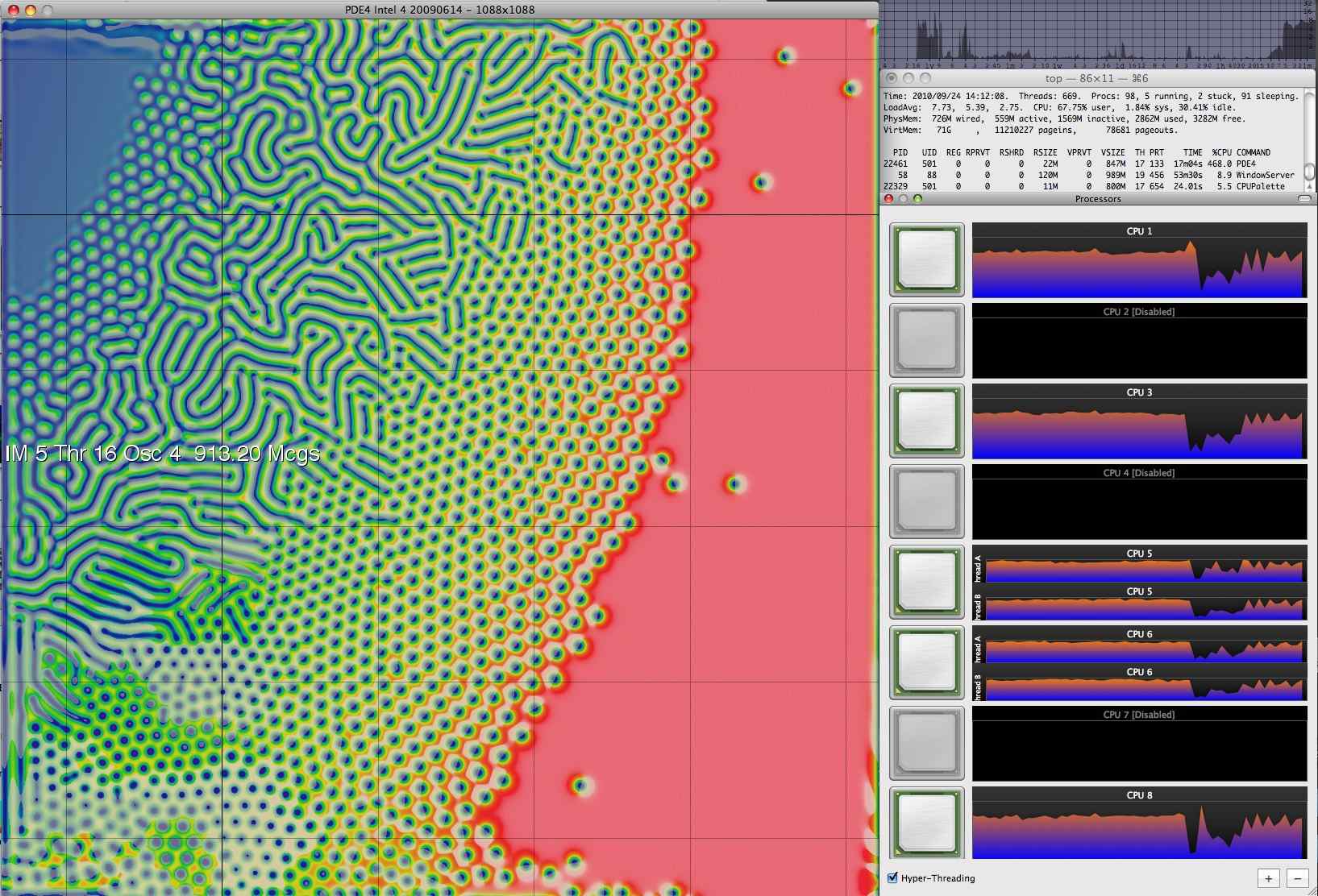
PDE4 on an 8-core Mac Pro with 5 cores and 7 threads enabled
I am continually looking for the next big chance to do more and better number-crunching, and I have written much on benchmarks (see for example my detailed work on how to compare all versions of the SPEC CPU Benchmarks).
This page was inspired by the Wikipedia page Timeline of Apple Macintosh models, and still draws from it heavily. I have added some non-Macintosh computers, made many of the dates more accurate, added details for recent models and an extensive section at the end that attempts to predict future developments.
| Year | Available | Model | Family | Announced2 | Discontinued | Details |
| 1976 | Apr | Apple 1 | Motherboard | 1976 April | 1977 | |
| 1977 | Jun 5 | Apple ][ | Desktop | 1977 Apr 16 | 1980 | |
| 1979 | Apple ][+4 | Desktop | 1979 | 1983 | ||
| 1980 | Jun | Apple /// | Desktop | 1980 May | 1985 | |
| 1983 | Jan | Lisa | All-In-One1 | 1983 Jan | 1985 Jan 1 | |
| Apple //e | Desktop | 1983 Jan | 1984 Jan | |||
| 1984 | Jan 24 | Lisa 2 | All-In-One1 | 1984 Jan 24 | 1985 Mar | |
| Apr? | Macintosh 128K4 | Compact AiO1 | 1984 Jan 24 | 1985 Jan 10 | ||
| Apr | Apple //c | Portable | 1984 Apr | |||
| Sep? | Macintosh 512K | Compact AiO1 | 1984 Sep 10 | 1986 Apr 14 | ||
| 1985 | Jan | Macintosh XL | Compact AiO1 | 1985 Jan 1 | 1986 Aug 1 | |
| Mar | Apple //e enhanced | Desktop | 1985 Mar | 1993 | ||
| 1986 | Jan | Macintosh Plus | Compact AiO1 | 1986 Jan 16 | 1990 Oct 15 | |
| Apr | Macintosh 512Ke4 | Compact AiO1 | 1986 Apr 14 | 1987 Oct 1 | ||
| Sep | Apple IIGS | Desktop | 1986 Jan 16 | 1992 Dec | ||
| 1987 | Mar | Macintosh SE | Compact AiO1 | 1987 Feb 3 | 1989 Aug 1 | |
| Mar | Macintosh II | Desktop | 1987 Mar 2 | 1990 Jan 15 | ||
| 1988 | Sep | Macintosh IIx | Desktop | 1988 Sep 19 | 1990 Oct 15 | |
| ? | Apple //c plus | Portable | 1988 Sep | 1990 Nov | ||
| 1989 | Jan 19 | Macintosh SE/30 | Compact AiO1 | 1989 Jan 19 | 1991 Oct 21 | |
| Mar 7 | Macintosh IIcx | Desktop | 1989 Mar 7 | 1991 Mar 11 | ||
| Aug 1 | Macintosh SE FDHD | Compact AiO1 | 1989 Aug 1 | 1990 Oct 15 | ||
| Sep 20 | Macintosh IIci | Desktop | 1989 Sep 20 | 1993 Feb 20 | ||
| Macintosh Portable | Portable | 1989 Sep 20 | 1991 Feb 11 | |||
| 1990 | Mar 19 | Macintosh IIfx | Desktop | 1990 Mar 19 | 1992 Apr 15 | |
| Oct 15 | Macintosh LC | Desktop | 1990 Oct 15 | 1992 Mar 23 | ||
| Macintosh Classic | Compact AiO1 | 1990 Oct 15 | 1992 Sep 14 | |||
| Macintosh IIsi4 | Desktop | 1990 Oct 15 | 1993 Mar 15 | |||
| 1991 | Feb 11 | Macintosh Portable (backlit screen) | Portable | 1991 Feb 11 | 1991 Oct 21 | |
| Oct 21 | Macintosh Classic II | Compact AiO1 | 1991 Oct 21 | 1993 Sep 13 | ||
| Quadra 700 | Desktop | 1991 Oct 21 | 1993 Mar 15 | |||
| Quadra 900 | Desktop | 1991 Oct 21 | 1992 May 18 | |||
| PowerBook 100 | Consumer Portable | 1991 Oct 21 | 1992 Aug 3 | |||
| PowerBook 1404 | Pro Portable | 1991 Oct 21 | 1992 Aug 3 | |||
| PowerBook 170 | Pro Portable | 1991 Oct 21 | 1992 Oct 19 | |||
| 1992 | Mar 23 | Macintosh LC II | Desktop | 1992 Mar 23 | 1993 Mar 15 | |
| May 18 | Quadra 950 | Desktop | 1992 May 18 | 1995 Oct 14 | ||
| Aug 3 | PowerBook 145 | Portable | 1992 Aug 3 | 1993 Jul 7 | ||
| Oct 19 | Macintosh IIvi | Desktop | 1992 Oct 19 | 1993 Feb 10 | ||
| Macintosh IIvx | Desktop | 1992 Oct 19 | 1993 Oct 10 | |||
| PowerBook 160 | Portable | 1992 Oct 19 | 1993 Aug 16 | |||
| PowerBook 180 | Portable | 1992 Oct 19 | 1994 May 16 | |||
| PowerBook Duo 210 | Portable | 1992 Oct 19 | 1993 Oct 21 | |||
| PowerBook Duo 230 | Portable | 1992 Oct 19 | 1994 Jul 27 | |||
| 1993 | Feb 10 | Macintosh LC III / III+ | Desktop | 1993 Feb 10 | 1994 Feb 14 | |
| Macintosh Color Classic | Compact AiO1 | 1993 Feb 10 | 1994 May 16 | |||
| Centris 610 | Desktop | 1993 Feb 10 | 1993 Oct 21 | |||
| Centris 650 | Desktop | 1993 Feb 10 | 1993 Oct 21 | |||
| Quadra 800 | Desktop | 1993 Feb 10 | 1994 Mar 14 | |||
| PowerBook 165c | Portable | 1993 Feb 10 | 1993 Dec 13 | |||
| Mar 22 | Workgroup Server 80 | Server | 1993 Mar 22 | 1995 Oct 17 | ||
| Workgroup Server 95 | Server | 1993 Mar 22 | 1995 Apr 3 | |||
| Jun 7 | PowerBook 145b | Portable | 1993 Jun 7 | 1994 Jul 18 | ||
| PowerBook 180c | Portable | 1993 Jun 7 | 1994 Mar 14 | |||
| Jun 28 | Macintosh LC 520 | Desktop | 1993 Jun 28 | 1994 Feb 2 | ||
| Jul 26 | Workgroup Server 60 | Server | 1993 Jul 26 | 1995 Oct 17 | ||
| Jul 29 | Centris / Quadra 660AV4 | Desktop | 1993 Jul 29 | 1994 Sep 12 | ||
| Quadra 840AV | Desktop | 1993 Jul 29 | 1994 Jul 18 | |||
| Aug 16 | PowerBook 165 | Portable | 1993 Aug 16 | 1994 Jul 18 | ||
| Oct 10 | Macintosh Color Classic II | Compact AiO1 | 1993 Oct 10 | 1995 Nov 1 | ||
| Oct 21 | Macintosh TV | Desktop | 1993 Oct 21 | 1995 Feb 1 | ||
| Quadra 605 | Desktop | 1993 Oct 21 | 1994 Oct 17 | |||
| Quadra 610 | Desktop | 1993 Oct 21 | 1994 Jul 18 | |||
| Quadra 650 | Desktop | 1993 Oct 21 | 1994 Sep 12 | |||
| PowerBook Duo 250 | Portable | 1993 Oct 21 | 1994 May 16 | |||
| PowerBook Duo 270c | Portable | 1993 Oct 21 | 1994 May 16 | |||
| 1994 | Feb 2 | Macintosh LC 550 | Desktop | 1994 Feb 2 | 1995 Mar 23 | |
| Macintosh LC 575 | Desktop | 1994 Feb 2 | 1995 Apr 3 | |||
| Mar 14 | Power Macintosh 61004 | Desktop | 1994 Mar 14 | 1996 May 18 | ||
| Power Macintosh 7100 | Desktop | 1994 Mar 14 | 1996 Jan 6 | |||
| Power Macintosh 8100 | Desktop | 1994 Mar 14 | 1996 Aug 14 | |||
| Apr 26 | Workgroup Server 6150 | Server | 1994 Apr 26 | 1995 Oct 1 | ||
| Workgroup Server 8150 | Server | 1994 Apr 26 | 1996 Feb 26 | |||
| Workgroup Server 9150 | Server | 1994 Apr 26 | 1996 Feb 26 | |||
| May 16 | PowerBook 520/c | Portable | 1994 May 16 | 1995 Sep 16 | ||
| PowerBook 540/c | Portable | 1994 May 16 | 1995 Aug 16 | |||
| PowerBook 550 | Portable | 1994 May 16 | 1996 Apr 1 | |||
| PowerBook Duo 280/c | Portable | 1994 May 16 | 1994 Nov 14 | |||
| Jul 18 | Quadra 630 | Desktop | 1994 Jul 18 | 1995 Apr 17 | ||
| PowerBook 150 | Portable | 1994 Jul 18 | 1995 Oct 14 | |||
| 1995 | Jan 28 | Power Macintosh 6200 / 6300 | Desktop | 1995 Jan 28 | 1996 Oct 17 | |
| Apr 3 | Macintosh LC 580 | Desktop | 1995 Apr 3 | 1995 Oct 1 | ||
| Performa 5200 | Desktop | 1995 Apr 3 | 1996 Oct 1 | |||
| Jun 19 | Power Macintosh 9500 | Desktop | 1995 Jun 19 | 1997 Feb 17 | ||
| Aug 7 | Power Macintosh 7200 | Desktop | 1995 Aug 7 | 1996 Apr 1 | ||
| Power Macintosh 7500 | Desktop | 1995 Aug 7 | 1997 Feb 17 | |||
| Power Macintosh 8500 | Desktop | 1995 Aug 7 | 1997 Feb 17 | |||
| Aug 28 | PowerBook 190 | Pro Portable | 1995 Aug 28 | 1996 Sep 1 | ||
| PowerBook 5300 | Portable | 1995 Aug 28 | 1996 Sep 1 | |||
| PowerBook Duo 2300c | Portable | 1995 Aug 28 | 1997 Feb 1 | |||
| 1996 | Feb 15 | Apple Network Server 500 | Server | 1996 Feb 15 | 1997 Apr 1 | |
| Apple Network Server 700/150 | Server | 1996 Feb 15 | 1997 Apr 1 | |||
| Feb 26 | Workgroup Server 7250 | Server | 1996 Feb 26 | 1997 Apr 21 | ||
| Workgroup Server 8550 | Server | 1996 Feb 26 | 1997 Apr 21 | |||
| Mar 10 | Performa 5260 / 5300 | Desktop | 1996 Mar 10 | 1997 Apr 1 | ||
| Apr 1 | Performa 5400 | Desktop | 1996 Apr 1 | 1997 Feb 17 | ||
| Power Macintosh 7600 | Desktop | 1996 Apr 1 | 1997 Oct 1 | |||
| Oct 16 | Apple Network Server 700/200 | Network Server | 1996 Oct 16 | 1997 Apr 1 | ||
| Oct 17 | Performa 6360 | Desktop | 1996 Oct 17 | 1997 Oct 1 | ||
| Oct 23 | Performa 6400 | Desktop | 1996 Oct 23 | 1997 May 1 | ||
| Nov 15 | Power Macintosh 4400 | Desktop | 1996 Nov 15 | 1997 Oct 11 | ||
| Nov 20 | PowerBook 1400 | Portable | 1996 Nov 20 | 1998 May 6 | ||
| 1997 | Feb 17 | Power Macintosh 5500 | Desktop | 1997 Feb 17 | 1998 Mar 31 | |
| Power Macintosh 6500 | Desktop | 1997 Feb 17 | 1998 Mar 14 | |||
| Power Macintosh 7300 | Desktop | 1997 Feb 17 | 1997 Nov 10 | |||
| Power Macintosh 8600 | Desktop | 1997 Feb 17 | 1998 Feb 17 | |||
| Power Macintosh 9600 | Desktop | 1997 Feb 17 | 1998 Mar 17 | |||
| PowerBook 3400 | Portable | 1997 Feb 17 | 1998 Mar 14 | |||
| Mar 19 | Twentieth Anniversary Macintosh | All-in-One1 | 1997 Mar 19 | 1998 Mar 14 | ||
| Mar 24 | Newton Messagepad 2000 | PDA3 | 1997 Mar 24 | ? | ||
| Apr? | eMate 300 | PDA3 | 1997 Jan 7 | |||
| Apr 21 | Workgroup Server 7350 | Server | 1997 Apr 21 | 1998 Mar 2 | ||
| Workgroup Server 9650 | Server | 1997 Apr 21 | 1998 Mar 2 | |||
| May 8 | PowerBook 2400c | Portable | 1997 May 8 | 1998 Mar 14 | ||
| Nov 10 | Power Macintosh G3 desktop | Pro Desktop | 1997 Nov 10 | 1999 Jan 5 | ||
| Power Macintosh G3 minitower | Pro Desktop | 1997 Nov 10 | 1999 Jan 5 | |||
| PowerBook G3 | Pro Portable | 1997 Nov 10 | 1998 Mar 14 | |||
| 1998 | Jan 31 | Power Macintosh G3 AIO | All-in-One1 | 1998 Jan 31 | 1998 Oct 17 | |
| Mar 2 | Macintosh Server G3 | Server | 1998 Mar 2 | 1999 Jan 1 | ||
| May 6 | PowerBook G3 series | Pro Portable | 1998 May 6 | 1999 May 10 | ||
| Aug 15 | iMac | Consumer Desktop | 1998 Aug 15 | 1999 May 10 | ||
| 1999 | Jan 5 | Power Mac G3 (Blue & White)4 | Pro Desktop | 1999 Oct 13 | details | |
| May 10 | PowerBook G3 ("Lombard") | Pro Portable | 2000 Feb 16 | |||
| Aug 31 | Power Mac G3 (450 MHz) | Pro Desktop | 2000 Xxx xx | details | ||
| Jul 21 | iBook | Consumer Port. | 2000 Sep 13 | |||
| Oct 5 | iMac (slot loading) | Consumer Desktop | 2002 Jan 7 | |||
| Oct 13 | Power Mac G4 Graphite | Pro Desktop | 2001 Jul 18 | |||
| 2000 | Feb 16 | PowerBook ("Pismo") | Pro Portable | 2001 Jan 9 | ||
| Power Mac G4 500 | Pro Desktop | details | ||||
| Jul 19 | Power Macintosh G4 Cube | Compact Desktop | 2001 Jul 3 | |||
| Sep 13 | iBook (FireWire) | Consumer Port. | 2001 May 1 | |||
| 2001 | Jan 9 | Power Mac G4 (Digital Audio) | Pro Desktop | 2001 Jul 18 | details | |
| Jan 31 | PowerBook G4 Titanium | Pro Portable | 2001 Jan 9 | 2003 Sep 16 | ||
| Feb 28 | Power Mac G4 (667 and 733) | Pro Desktop | 2001 Jan 9 | 2001 Jul 18 | details | |
| May 1 | iBook (white) | Consumer Port. | 2003 Oct | |||
| Jul 18 | Power Mac G4 Quicksilver | Pro Desktop | 2002 Jan 28 | details | ||
| 2002 | Jan 7 | iMac G4 15"4 | Consumer Desktop | 2004 Feb 4 | details | |
| Jan 28 | Power Mac G4 Quicksilver | Pro Desktop | 2002 Aug 13 | details | ||
| iBook (14") | Consumer Port. | 2003 Oct 22 | ||||
| Apr 29 | eMac | Consumer Desktop | sometime after 2006 Jul 3 | |||
| May 14 | Xserve | Rackmount Server | 2003 Feb 10 | |||
| Jul 17 | iMac G4 17"4 | Consumer Desktop | 2002 Jul 17 | 2003 Feb 4 | details | |
| Aug 13 | Power Macintosh G4 MDD | Pro Desktop | 2003 Jan 28 | details | ||
| 2003 | Jan 7 | PowerBook G4 Aluminum (12") | Pro Portable | 2006 May 16 | ||
| PowerBook G4 Aluminum (17") | Pro Portable | 2006 Apr 24 | ||||
| Jan 28 | Power Macintosh G4 (FW 800) | Pro Desktop | 2003 Jun 23 | details | ||
| Feb 4 | iMac G4 (X Only) | Consumer Desktop | 2003 Feb 4 | 2003 Sep 8 | details | |
| Feb 10 | Xserve slot loading | Rackmount Server | 2004 Jan 6 | |||
| Xserve Cluster Node | Rackmount Server | 2004 Jan 6 | ||||
| Jun 23 | Power Mac G5 | Pro Desktop | 2004 Jun 9 | details | ||
| Sep 9 | iMac G4 (USB 2.0) | Consumer Desktop | 2004 Jul 1 | details | ||
| Sep 16 | PowerBook G4 Aluminum (15") | Pro Portable | 2006 Feb 14 | |||
| Oct 22 | iBook G4 (12"/14")4 | Consumer Port. | 2006 May 16 | details | ||
| Nov 18 | iMac G4 20" | Consumer Desktop | 2004 Aug 31 | details | ||
| Power Mac G5 Dual 1.8 | Pro Desktop | 2004 Jun 9 | ||||
| 2004 | Jan 6 | Xserve G5 | Rackmount Server | 2006 Aug 7 | ||
| Xserve Cluster Node G5 | Rackmount Server | 2006 Aug 7 | ||||
| Jun 9 | Power Mac G5 (PCI-X 2)4 | Pro Desktop | 2005 Apr 27 | details | ||
| Aug 31 | iMac G5 | Consumer Desktop | 2005 May 3 | details | ||
| Oct 19 | Power Mac G5 Single | Pro Desktop | 2005 Apr 27 | details | ||
| 2005 | Jan 11 | Mac mini (original) | Compact Desktop | 2005 Sep 27 | details | |
| Apr 27 | Power Mac G5 | Pro Desktop | 2005 Oct 19 | details | ||
| May 3 | iMac G5 (ALS) | Consumer Desktop | 2005 Oct 12 | details | ||
| Sep 27 | Mac Mini (1.33/1.5) | Compact Desktop | details | |||
| Oct 12 | iMac G5 (iSight) | Consumer Desktop | 2006 Jan 10 | details | ||
| Oct 19 | Power Mac G5 Quad | Pro Desktop | 2006 Aug 7 | details | ||
| 2006 | Jan 10 | iMac Core Duo (17" / 20") | Consumer Desktop | 2006 Sep 6 | details | |
| never | MacBook Pro (15" 1.67 GHz) | Pro Portable | 2006 Jan 10 | 2006 Feb 14 | details | |
| Feb 14 | MacBook Pro (15") | Pro Portable | 2006 Jan 10 | 2008 Feb 26 | details | |
| Feb 28 | Mac mini (Intel Core Solo) | Compact Desktop | 2006 Sep 6 | details | ||
| Feb 28 | Mac mini (Intel Core Duo) | Compact Desktop | 2007 Aug 7 | details | ||
| Apr 24 | MacBook Pro (17") | Pro Portable | 2006 Oct 2x | details | ||
| May 16 | MacBook | Consumer Port. | 2006 Nov 0x | |||
| Aug 7 | Mac Pro (Woodcrest) | Pro Desktop | 2008 Jan 8 | details | ||
| Aug 7 | XServe (Intel) | Rackmount Server | 2008 Jan 8 | |||
| Sep 6 | Mac mini | Compact Desktop | details | |||
| Sep 6 | iMac | Consumer Desktop | 2007 Aug 7 | details | ||
| Oct 24 | MacBook Pro (Core 2 Duo)4 | Pro Portable | 2007 Jun 5 | details | ||
| Nov 0x | MacBook (Core 2 Duo) | Consumer Port. | 2008 Feb 26 | |||
| 2007 | Apr 4 | Mac Pro 8-core Clovertown | Pro Desktop | 2008 Jan 8 | details | |
| Jun 5 | MacBook Pro Santa Rosa | Pro Portable | 2008 Feb 26 | details | ||
| Jun 29 | iPhone (original) | PDA3 | 2007 Jan 9 | |||
| Aug 7 | iMac (aluminum enclosure) | Consumer Desktop | 2008 Apr 28 | details | ||
| Aug 7 | Mac mini (Core 2 Duo) | Compact Desktop | details | |||
| Nov 1 | MacBook Pro 2.6 GHz | Pro Portable | details | |||
| 2008 | Jan 8 | XServe Harpertown | Rackmount Server | |||
| Jan 8 | Mac Pro Harpertown | Pro Desktop | details | |||
| Jan 15 | MacBook Air | Consumer Port. | ||||
| Feb 26 | MacBook Penryn | Consumer Port. | ||||
| Feb 26 | MacBook Pro Penryn | Pro Portable | details | |||
| Apr 28 | iMac (Penryn) | Consumer Desktop | details | |||
| Jul 28 | iPhone 3G | PDA3 | 2008 Jun 9 | |||
| Oct 14 | MacBook Pro 15 (unibody) | details | ||||
| 2009 | Jan 6 | MacBook Pro 17 (unibody) | 2009 Jun 8 | details | ||
| Mar 3 | MacBook Pro 15 | 2009 Jun 8 | details | |||
| Mar 3 | Mac mini | Compact Desktop | details | |||
| Mar 3 | iMac (early 2009) | Consumer Desktop | details | |||
| Mar 3 | Mac Pro Nehalem4 | Pro Desktop | details | |||
| Jun 8 | MacBook Pro (SD card slot) | 2010 Apr 13 | details | |||
| Oct 20 | iMac (21.5 / 27) | Consumer Desktop | details | |||
| Oct 20 | Mac mini | Compact Desktop | details | |||
| Dec 4 | Mac Pro (late 2009) | Pro Desktop | details | |||
| 2010 | Apr 13 | MacBook Pro (mid 2010) | details | |||
| Jun 15 | Mac mini (unibody) | Compact Desktop | details | |||
| Jul 27 | iMac (ATI graphics) | Consumer Desktop | details | |||
| Aug 20 | Mac Pro Westmere | Pro Desktop | details | |||
| Oct 20 | MacBook Pro (2.8 option) | details | ||||
| 2011 | Feb 24 | MacBook Pro (Sandy Bridge)4 | details | |||
| May 3 | iMac Sandy Bridge | Consumer Desktop | details | |||
| 2012 | Jun 11 | Mac Pro "Meh" | Pro Desktop | details | ||
| Possible | Future Developments |
Details of Certain Specific Systems
These details are provided for the following purposes:
- To detail the specifications of the PCMS (processor, cache and memory system) which constitute most of the variation in system-level CPU benchmarks.
- Links to web pages for even more specs if you want it.
- Showing when the chip vendor (e.g. Intel) made the product available and their announced price. Future systems will probably be based on new CPUs with similar prices and with a similar delay after CPU release date. For portables and Mac Mini, wattage (TDP) is also a consderation. Using these criteria it is easy to predict that, for example, Apple will not use the first set of 6-core "Dunnington" processors because they cost too much (except possibly in XServe as a BTO for a new Cluster Node offering).
CPU: "G4" PowerPC 7447a at 1.25 GHz or 1.42 GHz
L2-Cache: 512K
Bus: 167 MHz
Memory: 333 MHz PC2700 DDR SDRAM
EveryMac profiles: 1.25 GHz, 1.42 GHz
CPU: "G4" PowerPC 7447a at 1.33 GHz or 1.5 GHz
L2-Cache: 512K
Bus: 167 MHz
Memory: 333 MHz PC2700 DDR SDRAM
EveryMac profiles: 1.33 GHz, 1.5 GHz
CPU: Intel "Yonah" Core Solo T1200 (1.5 GHz) or Core Duo T2300 (1.66 GHz)
L2-Cache: 2M
Bus: 667 MHz
Memory: 667 MHz PC2-5300 DDR2 SDRAM
CPU: "Yonah" Core Duo T2300 (1.66 GHz) or T2400 (1.83 GHz)
L2-Cache: 2M
Bus: 667 MHz
Memory: 667 MHz PC2-5300 DDR2 SDRAM
CPU: "Yonah" Core Duo T5600 (1.83 GHz) or T7200 (2.0 GHz)
L2-Cache: 2M
Bus: 667 MHz
Memory: 667 MHz PC2-5300 DDR2 SDRAM
CPU: "Penryn" Core 2 Duo P7350 (2.0 GHz) or P8400 (2.26 GHz)
L2-Cache: 3M
Bus: 1.066 GT/sec
Memory: 1.066 GHz PC3-8500 DDR3 SDRAM
CPU: "Penryn" Core 2 Duo P7550 (2.26 GHz), P8700 (2.53 GHz), or P8800 (2.66 GHz)
L2-Cache: 3M
Bus: 1.066 GT/sec
Memory: 1.066 GHz PC3-8500 DDR3 SDRAM
Mac Mini ("Unibody", June 2010)
CPU: "Penryn" Core 2 Duo P8600 (2.4 GHz) or P8800 (2.66 GHz)
L2-Cache: 3M
Bus: 1.066 GT/sec
Memory: 1.066 GHz PC3-8500 DDR3 SDRAM
iMac G4 (original with 15" screen), 2002 Jan 7 **
CPU: "G4" PowerPC 7441 at 700 MHz or 7445 at 800 MHz
L2-Cache: 256K
Bus: 100 MT/sec
Memory: PC133 SDRAM (133 MT/sec)
EveryMac profiles: 700 MHz, 800 MHz
iMac G4 (17" screen), 2002 Jul 17 **
CPU: "G4" PowerPC 7445 at 800 MHz
L2-Cache: 256K
Bus: 100 MT/sec
Memory: PC133 SDRAM (133 MT/sec)
CPU: "G4" PowerPC 7445 at 800 MHz or 1.0 GHz
L2-Cache: 256K
Bus: 100 or 133 MT/sec
Memory: PC133 (133 MT/sec) or PC2100 (266 MT/sec) SDRAM
EveryMac profiles: 800 MHz, 1.0 GHz
iMac G4 (USB 2), 2003 Sep 8 and Nov 18
CPU: "G4" PowerPC 7445 at 1.0 or 1.25 GHz
L2-Cache: 256K
Bus: 167 MT/sec
Memory: PC2700 (333 MT/sec) SDRAM
EveryMac profiles: 15" 1.0 GHz, 17" 1.25 GHz, 20" 1.25 GHz
CPU: "G5" PowerPC 970 at 1.6 or 1.8 GHz
L2-Cache: 512K
Bus: 533 or 600 MT/sec
Memory: PC3200 (400 MT/sec) SDRAM
EveryMac profiles: 17" 1.6 GHz, 17" 1.8 GHz, 20" 1.8 GHz
CPU: "G5" PowerPC 970 (or 970fx) at 1.8 or 2.0 GHz
L2-Cache: 512K
Bus: 600 or 667 MT/sec
Memory: PC3200 (400 MT/sec) SDRAM
EveryMac profiles: 17" 1.8 GHz, 17" 2.0 GHz, 20" 2.0 GHz
CPU: "G5" PowerPC 970fx at 1.9 or 2.1 GHz
L2-Cache: 512K
Bus: 633 or 700 MT/sec
Memory: PC2-4200 (533 MT/sec) DDR2 SDRAM
EveryMac profiles: 17" 1.9 GHz, 20" 2.1 GHz
iMac (17" and 20" core 2), 2006 Jan 10
CPU: "Yonah" Core Duo T2400 (1.83 GHz) or T2500 (2.0 GHz) (2006 Jan 5: $294 or $423)
L2-Cache: 2M (shared by both cores)
Bus: 667 MT/sec
Memory: 667 MHz PC2-5300 DDR2 SDRAM
EveryMac profiles: 17-inch, 20-inch
iMac (17", 20" and 24" core 2), 2006 Sep 6
CPU: "Merom" Core 2 Duo T7200 (2.0 GHz), T7400 (2.16 GHz) or T7600 (2.33 GHz) (2006 Aug 28: $294, $423, $637)
L2-Cache: 4M (shared by both cores)
Bus: 667 MT/sec
Memory: 667 MHz PC2-5300 DDR2 SDRAM
EveryMac profiles: 17" 2.0 GHz, 20" 2.16 GHz, 24" 2.33 GHz
There was also a model for education customers only, with a 1.83-GHz processor (Core 2 Duo T5600), and using Intel GMA 950 "integrated graphics". It was $899, but only for purchase by institutions (not even students or faculty). A profile is here.
CPU: "Merom" Core 2 Duo T7300 (2.0 GHz), T7700 (2.4 GHz) (2007 May 9: $241 or $530) or "Merom XE" Core 2 Extreme X7900 (2.8 GHz) (2007 Aug 22: $851)
L2-Cache: 4M (shared by both cores)
Bus: 800 MT/sec
Memory: 667 MHz PC2-5300 DDR2 SDRAM
EveryMac profiles: 20-inch 2.0 GHz, 24-inch 2.4 GHz, 24-inch 2.8 GHz
CPU: "Penryn" Core 2 Duo E8135 (2.4 GHz), O
E8335 (2.67 GHz), E8235 (2.8 GHz) or "Penryn XE" Core 2 Duo E8435 (3.06 GHz) (prices unknown)
L2-Cache: 6M (shared by both cores)
Bus: 1066 MT/sec (2.8 GHz model)
Memory: 800 MHz PC2-6400 DDR2 SDRAM
EveryMac profiles: 20-inch 2.4 GHz, [20-inch 2.67 GHz| [24-inch 2.8 GHz| 24-inch 3.06 GHz
CPU: "Penryn" Core 2 Duo E8135 (2.66 GHz), E8335 (2.93 GHz) or "Penryn XE" Core 2 Duo E8435 (3.06 GHz) (E8435 released 2008 Aug 10 at $266)
Cores/Threads: All models have 2 cores and 2 threads.
L2-Cache: 6M (shared by both cores)
Bus: 1066 MT/sec
Memory: 1.066 GHz PC3-8500 DDR3 SDRAM
EveryMac profiles: 20-inch 2.66 GHz, 24-inch 2.66 GHz, 24-inch 2.93 GHz, 24-inch 3.06 GHz
On April 7 Apple added a 20-inch, 2.0-GHz model for education customers only. A profile courtesy of EveryMac can be found here. Its price was $899, but individuals could not buy it, even if they were students or faculty — it could only be bought by institutions.
CPU: "Penryn XE" Core 2 Duo E8435 (3.06 GHz) or E8600 (3.33 GHz) or "Lynnfield" Core i5 750 (2.66-3.2 GHz) or Core i7 860 (2.8-3.46 GHz) (i5 and i7 both released 2009 Sep 8 at $196 and $284)
Cores/Threads: "Core 2 Duo" models have 2 cores and 2 threads; "Core i5" model has 4 cores and 4 threads; "Core i7" model has 4 cores and 8 threads.
L2-Cache: 3M (on E8435), 6M (on E8600) or 8M (on Core i5 and i7) (shared by all cores)
Bus: 1066 MT/sec (2.8 GHz model)
Memory: 1.066 GHz PC3-8500 DDR3 SDRAM
EveryMac profiles: 21.5-inch 3.06 GHz, 21.5-inch 3.33 GHz, 27-inch 3.06 GHz, 27-inch 3.33 GHz, 27-inch Core i5, 27-inch Core i7
iMac (ATI graphics), 2010 Jul 27
CPU: "Clarkdale" Core i3 540 (3.06 GHz dual-core) or 550 (3.2 GHz dual-core) or "Lynnfield" Core i5 760 (2.8-3.33 GHz quad-core) or "Clarkdale" Core i5 680 (3.6-3.86 GHz dual-core) or "Lynnfield" Core i7 875K (2.93-3.6 GHz quad-core)
Cores/Threads: all "dual-core" models have 2 cores and 4 threads; "Core i5 quad-core" model has 4 cores and 4 threads; "Core i7" model has 4 cores and 8 threads.
L2-Cache: 2M per core (i.e. 4M or 8M total)
Bus: 1333 MT/sec
Memory: 1.333 GHz PC3-10600 DDR3 SDRAM
EveryMac profiles: 21.5-inch 3.06 GHz Core i3, 21.5-inch 3.2 GHz Core i3, 21.5-inch 3.6 GHz Core i5, 27-inch 3.2 GHz Core i3, 27-inch 2.8 GHz Core i5, 27-inch 3.6 GHz Core i5, 27-inch 2.93 GHz Core i7
iMac (Sandy Bridge), 2011 May 3
CPU: "Sandy Bridge" Core i5 2400S (2.5-3.3 GHz), 2500S (2.7-3.7 GHz) or 2400 (3.1-3.4 GHz) or "Sandy Bridge" Core i7 2600S (2.8-3.8 GHz) or 2600 (3.4-3.8 GHz)
Cores/Threads: all "Core i5" models have 4 cores and 4 threads; "Core i7" models have 4 cores and 8 threads.
L2-Cache: 6M (Core i5) or 8M (Core i7)
Bus: 5 GT/s
Memory: 1.333 GHz PC3-10600 DDR3 SDRAM
EveryMac profiles: 21.5-inch 2.5 GHz Core i5 21.5-inch 2.7 GHz Core i5 21.5-inch 2.8 GHz Core i7 27-inch 2.7 GHz Core i5 27-inch 3.1 GHz Core i5 27-inch 3.4 GHz Core i7
(This model was made available only to educational customers.)
CPU: "Sandy Bridge" Core i3 2100 (3.1 GHz, no turbo boost)
Cores/Threads: 2 cores and 4 threads
L2-Cache: 3M
Bus: 5 GT/s
Memory: 1.333 GHz PC3-10600 DDR3 SDRAM
EveryMac profiles: 21.5-inch 3.1 GHz Core i3
Details for iBook and MacBook
This was a new line created in 1999 as a consumer-oriented portable. It initially had a substantially different look and feel from the PowerBooks, but has gradually converged over the following 10 years.
CPU: "G4" PowerPC 7457 at 800 MHz (12" model) or 933 MHz (14" model)
L2-Cache: 256K
Bus: 133 MT/sec
Memory: PC2100 DDR SDRAM (267 MT/sec)
Details for Powerbook and MacBook Pro
The never-shipped 1.67 GHz MacBook Pro 15"
CPU: "Yonah" Core Duo L2400 (1.67 GHz) (2006 Jan 5: $316)
L2-Cache: 2M (shared by both cores)
Bus: 667 MT/sec
Memory: 667 MHz PC2-5300 DDR2 SO-DIMM
This system never shipped. On 2006 Feb 14, Apple announced that the MacBook Pro line (which had not yet shipped) would feature 1.83, 2.0 and 2.16 GHz processors, thus eliminating the 1.67 GHz version.
MacBook Pro, 2006 Feb 14 and 2006 Apr 24
CPU: "Yonah" Core Duo T2400 (1.83 GHz), T2500 (2.0 GHz) or T2600 (2.16 GHz) (2006 Jan 5: $294 - $637)
L2-Cache: 2M (shared by both cores)
Bus: 667 MT/sec
Memory: 667 MHz PC2-5300 DDR2 SO-DIMM
lowendmac profiles: 15-inch, 17-inch
CPU: "Merom" Core 2 Duo T7400 (2.16 GHz) or T7600 (2.33 GHz) (2006 Aug 28: $423, $637)
L2-Cache: 4M (shared by both cores)
Bus: 667 MT/sec
Memory: 667 MHz PC2-5300 DDR2 SDRAM
EveryMac's profiles: 2.16 15", 2.33 17"
lowendmac profiles: 15-inch, 17-inch
MacBook Pro (Santa Rosa), 2007 Jun 5
CPU: "Merom" Core 2 Duo T7500 (2.2 GHz) or T7700 (2.4 GHz) (2007 May 9: $316, $530)
L2-Cache: 4M (shared by both cores)
Bus: 800 MT/sec
Memory: 667 MHz PC2-5300 DDR2 SDRAM
lowendmac profiles: 15-inch 17-inch
EveryMac's profiles: 2.2 15'', 2.4 17''
MacBook Pro (17'' 2.6 GHz option), 2007 Nov 1
CPU: "Merom" Core 2 Duo T7800 (2.6 GHz) (2007 Sep 2: $530)
L2-Cache: 4M (shared by both cores)
Bus: 800 MT/sec
Memory: 667 MHz PC2-5300 DDR2 SDRAM
EveryMac's profile (which only makes brief mention of the 2.6 GHz version)
MacBook Pro (Penryn), 2008 Feb 26 (2.5 and 2.6 GHz versions)
CPU: "Penryn" Core 2 Duo T8300 (2.4 GHz) or T9300 (2.5 GHz) or T9500 (2.6 GHz) (2008 Jan 6: $241, $316, $530)
L2-Cache: 3M (2.4 GHz models) or 6M (faster models) (shared by both cores)
Bus: 800 MT/sec
Memory: 667 MHz PC2-5300 DDR2 SDRAM
lowendmac profiles: 15-inch 17-inch
EveryMac's profiles: 2.4 15'' 2.5 15'', 2.6 17'' (which mentions the 2.6 GHz option)
MacBook Pro 15'' (Unibody), 2008 Oct 14
CPU: "Penryn" Core 2 Duo P8600 (2.4 GHz) (2008 Jun 13: $241), T9400 (2.533 GHz) or T9600 (2.8 GHz) (both 2008 Jul 14: $316, $530)
L2-Cache: 3M (2.4 model) or 6M (higher models) (cache is shared by both cores)
Bus: 1.066 GT/sec
Memory: 1.066 GHz PC2-8500 DDR2 SDRAM
lowendmac profiles: 15-inch
NOTE: In 2008 Oct, the 17-inch MacBook Pro still had the same CPU, bus and memory specs as the 2008 Feb 26 version, but its screen and hard drive were changed in conjunction with the all-new "unibody" 15'' model.
MacBook Pro (17-inch Unibody, January 2009)
CPU: "Penryn" Core 2 Duo T9550 (2.66 GHz) or T9800 (2.93 GHz) ()
L2-Cache: 6M
Bus: 1.066 GT/sec
Memory: 1.066 GHz PC2-8500 DDR2 SDRAM
lowendmac profiles: 17-inch
EveryMac's profile: 2.66 17''
MacBook Pro (15-inch Unibody, March 2009)
CPU: "Penryn" Core 2 Duo T9550 (2.66 GHz) ()
L2-Cache: 6M
Bus: 1.066 GT/sec
Memory: 1.066 GHz PC2-8500 DDR2 SDRAM
EveryMac's profile: 2.66 15''
MacBook Pro (SD card slot, June 2009)
CPU: "Penryn" Core 2 Duo P8400 (2.26 GHz), P8700 (2.53 GHz), P8800 (2.66 GHz), T9600 (2.8 GHz), or T9900 (3.06 GHz) (20080714: $209 - $530)
Cores/Threads: All models have 2 cores and 2 threads.
L2-Cache: 3M (2.26, 2.53 and 2.66 GHz models) or 6M (2.8 and 3.06 GHz models)
Bus: 1.066 GT/sec
Memory: 1.066 GHz PC2-8500 DDR2 SDRAM
lowendmac profiles: 13-inch 15-inch 17-inch
EveryMac's profiles: 2.26 13'' 2.53 13'' 2.53 15'' 2.66 15'' 2.8 15'' 2.8 and 3.06 17''
CPU: "Penryn" Core 2 Duo P8600 (2.4 GHz) or P8800 (2.66 GHz) (20080613: $241)
or "Arrandale" Core i5 520M (2.4-2.93 GHz) or 540M (2.53-3.06 GHz) (20100107: $225, $257)
or "Arrandale" Core i7 620M (2.66-3.33 GHz) (20100107: $332)
Cores/Threads: All models have 2 cores; "Core 2 Duo" models have 2 threads; "Core i5" and "Core i7" models have 4 threads.
L2-Cache: 3M (Core 2 Duo and Core i5 models) or 4M (2.66 Core i7 model)
Bus: 1.066 GT/sec
Memory: 1.066 GHz PC3-8500 DDR3 SDRAM
EveryMac's profiles: 2.4 13'' 2.66 13'' 2.4 15'' 2.53 15'' 2.66 15'' 2.53 and 2.66 17''
MacBook Pro (2.8 GHz option), Oct 2010
CPU: "Arrandale" Core i7 640M (2.8-3.46 GHz) (20100926: $346)
Cores/Threads: 2 cores/4 threads.
L2-Cache: 4M
Bus: 1.066 GT/sec
Memory: 1.066 GHz PC3-8500 DDR3 SDRAM
CPU: 13'' models have "Sandy Bridge" Core i5 2410M (2.3-2.9 GHz), or Core i7 2620M (2.7-3.4 GHz) (20110221: $225, $346)
15'' and 17'' models have "Sandy Bridge" Core i7 2630QM (2.0-2.9 GHz), 2720QM (2.2-3.3 GHz) or 2820QM (2.3-3.4 GHz) (20110221: $378, $378, $568)
Cores/Threads: 13'' models have 2 cores and 4 threads; 15'' and 17'' models have 4 cores and 8 threads
L3-Cache: 3MB (13'' with Core i5), 4MB (13'' with Core i7), 6MB (2.0 GHz and 2.2 GHz quad-core), or 8MB (2.3 GHz quad-core)
Bus: 1.333 GT/sec
Memory: 1.333 GHz DDR3 SDRAM
lowendmac profiles: 13-inch 15-inch 17-inch
Idle Speculations on MacBook Pro
(none at present)
Details for PowerMac and Mac Pro
Power Mac G3 (Blue and White), 1999 Jan 5
CPU: IBM PowerPC 750 (300, 350 or 400 MHz)
L2-Cache: 512K (300 MHz model) or 1M (faster models)
Bus: 100 MHz
Memory: PC100 SDRAM
CPU: IBM PowerPC 750 (450 MHz)
L2-Cache: 1M
Bus: 100 MHz
Memory: PC100 SDRAM
Power Mac G4 "Gigabit Ethernet", 2000 Feb 16
CPU: 2x IBM PowerPC 750 (450 or 500 MHz)
L2-Cache: 2M (1M per processor)
Bus: 100 MHz
Memory: PC100 SDRAM
Power Mac G4 "Digital Audio", 2001 Jan 9
CPU: Motorola 7410 "Nitro" (single 466 MHz or dual 533 MHz)
L2-Cache: 1M (or 2M for dual 533 model)
Bus: 133 MHz
Memory: PC133 SDRAM
Power Mac G4 "Digital Audio", 2001 Feb
CPU: Motorola 7450 "V'ger" (667 or 733 MHz)
L2-Cache: 1M
Bus: 133 MHz
Memory: PC133 SDRAM
Power Mac G4 "Quicksilver", 2001 Jul 18
CPU: Motorola 7450 "V'ger" (733 or 867 MHz)
CPU: 2x Motorola 7450 "V'ger" (800 MHz)
L2-Cache: 1M (2M for dual 800 model)
Bus: 133 MHz
Memory: PC133 SDRAM
EveryMac profiles: 733, 867, dual 800
Power Mac G4 "Quicksilver", 2002 Jan 28
CPU: Motorola 7455 "Apollo 6" (800 or 933 MHz)
CPU: 2x Motorola 7455 "Apollo 6" (1.0 GHz)
L2-Cache: none on 800 MHz model; 2M on 933 MHz model; 4M (2M per processor) on 1.0 GHz model
Bus: 133 MHz
Memory: PC133 SDRAM
EveryMac profiles: 800, 933, dual 1.0
Power Mac G4 (Mirror Drive Doors), 2002 Aug 13
CPU: 2x Motorola 7455 "Apollo 6" (867 MHz, 1.0 GHz or 1.25 GHz)
L2-Cache: 1M (867 and 1.0 GHz models) or 2M (1.25 GHz model)
Bus: 133 MHz (867 model), 167 MHz (faster models)
Memory: 266 MHz PC2100 DDR SDRAM (867 model) or 333 MHz PC2700 DDR SDRAM (faster models)
EveryMac profiles: 867, 1.0, 1.25
Power Mac G4 (Firewire 800), 2003 Jan 28
CPU: Motorola 7455 "Apollo 6" (single 1.0 GHz, dual 1.25 or dual 1.42 GHz)
L2-Cache: 1M (1.0 GHz model), 2M (dual 1.25 GHz model), or 4M (dual 1.42 GHz model)
Bus: 133 MHz (1.0 GHz model), 167 MHz (faster models)
Memory: 266 MHz PC2100 DDR SDRAM (1.0 GHz model) or 333 MHz PC2700 DDR SDRAM (faster models)
EveryMac profiles: 1.0, 1.25, 1.42
CPU: IBM PowerPC 970 (single 1.6, single 1.8, or dual 2.0 GHz)
L2-Cache: 512K
Bus: 800 MHz, 900 Mhz or 1.0 GHz
Memory: 333 MHz PC2700 DDR RAM (1.6 GHz model) or 400 MHz PC3200 DDR RAM (faster models)
EveryMac profiles: 1.6, 1.8, 2.0
PowerMac G5 (PCI-X 2), 2004 Jun 9 **
CPU: 2x IBM PowerPC 970fx (1.8, 2.0 or 2.5 GHz)
L2-Cache: 1M (512K per CPU)
Bus: 900 Mhz, 1.0 GHz or 1.25 GHz
Memory: 400 MHz PC3200 DDR RAM
EveryMac profiles: 1.8, 2.0, 2.5
PowerMac G5 Single, 2004 Oct 19
CPU: IBM PowerPC 970fx (1.8 GHz)
L2-Cache: 512K
Bus: 600 Mhz
Memory: 400 MHz PC3200 RAM
CPU: 2x IBM PowerPC 970fx (2.0, 2.3 or 2.7 GHz)
L2-Cache: 1M (512K per CPU)
Bus: 1.0, 1.15 or 1.35 GHz
Memory: 400 MHz PC3200 DDR RAM
EveryMac profiles: 2.0, 2.3, 2.7
CPU: IBM PowerPC 970MP "Antares" (2.0 or 2.3 GHz)
L2-Cache: 2M (1M per core)
Bus: 1.0 or 1.15 GHz
Memory: 533 MHz PC2-4200 DDR2
CPU: 2x IBM PowerPC 970MP "Antares" (2.5 GHz)
L2-Cache: 4M (1M per core)
Bus: 1.25 GHz
Memory: 533 MHz PC2-4200 DDR2
CPU: 2x Intel Core 2 Duo "Woodcrest" 5130 (2.0 GHz), 5150 (2.66 GHz) or 5160 (3.0 GHz) (all 2006 Jun 26: $316 - $851)
L2-Cache: 8M (4M for each pair of cores)
Bus: 1.33 GT/sec
Memory: 667 MHz PC2-5300 DDR2 fully buffered (FB-DIMM) ECC RAM, dual channel (10.7 GB/s bandwidth)
CPU: 2x Intel Core 2 Quad "Clovertown" X5365 (3.0 GHz) (2007 April 4: $1350)
L2-Cache: 16M (each pair of cores shares 4M)
Bus: 1.33 GT/sec
Memory: 667 MHz PC2-5300 DDR2 fully buffered (FB-DIMM) ECC RAM, dual channel (10.7 GB/s bandwidth)
CPU: 2x Intel Core 2 Quad "Harpertown" E5462 (2.8 GHz), E5472 (3.0 GHz) or X5482 (3.2 GHz) (all 2007 Nov 11: $797 or 851, $958, $1279)
Cores/Threads: All models have 8 cores and 8 threads.
L2-Cache: 24M (each pair of cores shares 6M)
Bus: 1.6 GT/sec
Memory: 800MHz DDR2 ECC fully buffered DIMM (FB-DIMM) RAM, dual channel (12.8 GB/s bandwidth)
Mac Pro "Gainestown Nehalem", 2009 Mar 3 **
CPU: 1x Xeon W3520 (2.66 GHz) or W3540 (2.93 GHz) ($284, $562)
or 2x Xeon E5520 (2.26 GHz), X5550 (2.66 GHz) or X5570 (2.93 GHz) ($373 - $1386)
Cores/Threads: Each Xeon CPU has 4 cores and 8 threads; thus the dual-CPU machines have 8 cores and 16 threads.
Cache: 256K L2 and 2M L3 per core (1 processor = 4 cores, i.e. either 9M or 18M total cache)
Bus: Controls memory directly; uses QuickPath Interconnect at 5.86 GT/sec (2.26 GHz 8-core model) or 6.4 GT/sec (all other models) for data transfer between one processor and the other, and between processor(s) and the video, hard drives and rest of the system.
Memory: 1066 MHz DDR3 ECC SDRAM, triple channel (25.6 GB/s bandwidth per CPU socket)
EveryMac profiles: Quad 2.66, Octo-core 2.26.
Mac Pro (late 2009 3.33 GHz), 2009 Dec 4
CPU: 1x Xeon X5590 (3.33 GHz) ($1600)
Cores/Threads: 4 physical cores, 8 threads.
Cache: 256K L2 and 2M L3 per core (1 processor = 4 cores, i.e. 9M total cache)
Bus: Controls memory directly; uses QuickPath Interconnect at 6.4 GT/sec for data transfer between one processor and the other, and between processor(s) and the video, hard drives and rest of the system.
Memory: 1066 MHz DDR3 ECC SDRAM, triple channel (25.6 GB/s bandwidth)
Mac Pro "Westmere", 2010 August
CPU: 1x Xeon W3530 (2.8 GHz 4-core), W3565 (3.2 GHz 4-core) or W3680 (3.33 GHz 6-core) ($unknown, $562, $999)
or 2x Xeon E5620 (2.4 GHz 4-core), X5650 (2.66 GHz 6-core) or X5670 (2.93 GHz 6-core) ($387, $996, $1440)
Cores/Threads: From 4 to 12 cores, with 2 threads per core.
Cache: most models have 256K L2 and 2M L3 per core (i.e. from 9M to 27M total cache); the 8-core (2x Xeon E5620) model has 256K L2 and 3M L3 cache per core (26M total cache).
Bus: Controls memory directly; uses QuickPath Interconnect at 4.8 GT/sec (2.8 GHz 4-core model), 5.86 GT/sec (2x 2.4 GHz 4-core) or 6.4 GT/sec (6-core and 12-core models) for data transfer between one processor and the other, and between processor(s) and the video, hard drives and rest of the system.
Memory: 1066 MHz DDR3 ECC SDRAM (4-core and 6-core systems)
or 1333 MHz DDR3 ECC SDRAM (8-core and 12-core systems)
triple channel (25.6 GB/s or 32 GB/s bandwidth per CPU socket)
(After nearly two years, Apple updated its Mac Pro lineup ever so slightly: the 4-core entry system went from 2.8 GHz to 3.2 GHz (still $2500), and the top 12-core model went from 2.93 GHz up to 3.06 GHz (still $6200). Here is a news story about the 2012 changes: Apple incrementally updates Mac Pro desktop for 2012)
CPU: 1x Xeon W3565 (3.2 GHz 4-core) or W3680 (3.33 GHz 6-core) ($562, $999) or 2x Xeon E5645 (2.4 GHz 6-core), X5650 (2.66 GHz 6-core) or X5675 (3.06 GHz 6-core) ($551, $996, $1440) All other specs are the same as above. Note there is no longer an 8-core model.
Mac Pro "Ivy Bridge", 2013 Dec 19
CPU: 1x Xeon E5-1620v2 (3.7-3.9 GHz) or E5-1650v2 (3.5-3.9 GHz)
or E5-1680v2 (3.0-3.9 GHz) or E5-2697v2 (2.7-3.5 GHz)
($294 - $2614)
Cores/Threads: 4, 6, 8 or 12 cores, number of threads is twice as much
Cache: 256K L2 per core; 10M, 12M, 25M or 30M of L3 cache.
Bus: None (Controls memory and PCI directly)
Memory: DDR3-1866 (PC3-15000) ECC SDRAM, quad channel (total bandwidth 59.7 GB/s)
EveryMac profiles: 4-core 6-core 8-core 12-core
Idle Speculations for Mac Pro
The Situation in 2012 (speculation)
(written in 2012 June)
Lately there has been a lot of speculation that Apple would soon drop the Pro line entirely. Apple answered these doubts by making small changes to the CPU speeds of the lowest and highest Mac Pro models, while keeping the price structure the same. The fastest 12-core option uses the Xeon X5675, which Intel released in February 2011. Although it was released after the desktop Sandy Bridge processors, the Xeon X5675 is still a Westmere chip.
Intel has (in late 2011) updated its Xeon line to include Sandy Bridge, but the new Sandy Bridge Xeons provide no integrated Thunderbolt or USB 3.0 capability. This effectively makes it impossible for Apple to bring these upgrades (present on the MacBook Pro since the 2011 March models) to the Xeon-based Mac Pro.
Dual-Socket Workstations Similar to Mac Pro
This chart summarizes dates, prices, and performance figures for two-socket servers or workatations using the same Intel processors as Apple has used in most of its "middle-priced" Mac Pro. In each case:
- I chose processors identical to what Apple offered in Mac Pros (as seen above) extending forward to Sandy Bridge-EP to show what might have been possible if Apple had chosen to use those processors.
- I tried to choose processors that cost about $1000 each
- The date given is the date of the first SPEC benchmark result for a system with the given processor configuration
- The SPEC benchmark figures are weighted averages of all of the SPEC results for workstations and servers with two of the indicated Xeon processors
|
Apple's Special Relationship With Intel
On several occasions it has been clear that Apple has been able to get certain part numbers from Intel a little ahead of the rest of the industry. Recent examples include:
- 2007 Jan: The Pentium M "Crofton" used in Apple TV (see macnn [24]).
- 2007 Apr 4: The 3.0 GHz Xeon X5365 "Clovertown" used in the first 8-core Mac Pro (see electronista [25]).
- 2008 Apr 29: The 3.07 GHz Core 2 Extreme X9100 "Penryn", used in the top-model iMac months before being released to the general market on July 14. (see TG Daily [33]).
- 2008 Jan: The original MacBook Air's 1.6 and 1.8 GHz processors (described by Anand: [29] and [30]).
- 2009 Mar 3: The first Nehalem-based Mac Pros, using Xeon processors (the W3520, W3540, E5520, X5550 and X5570 or (by some accounts) X5580) about 3 weeks before being available to the general market (see TG Daily [55]).
Before Apple became a major customer of Intel, a similar type of relationship existed with IBM regarding the PowerPC G5 (the 970, 970FX, and 970MP).
In May 2011, a special Apple-Intel relationship was confirmed directly [90] by Intel's Tom Kilroy, who stated:
"We work very closely with them and we're constantly looking down the road at what we can be doing relative to future products. I'd go as far as to say Apple helps shape our roadmap"
More recently, Apple has been cited[107] as the reason for Intel adding much better integrated graphics (branded "HD Graphics 3000") to its mobile Sandy Bridge (2nd-Generation Core) processors, and similar even better-performing graphics to subsequent products, culminating with the 128 MiB eDRAM cache for the 4-core variants of Haswell with "Iris Pro 5200 Graphics", which were used in the late 2013 refresh of the 15-inch Retina MacBook Pro.
Appendix A: Charts and Tables
Charts and Tables of Intel-CPU-Specific History
Tick Tock Chart
This chart illustrates the general pattern of alternation between the development of semiconductor processes (see the lithography table below) and changes in computer architecture, illustrated by the past 20 years of Intel CPU history. Though Intel attached the "Tick-Tock" marketing to it in 2007, the practice (motivated mainly by risk-reduction and yield-based economics) is common throughout the industry and began long before Intel made it "a thing".
The cadence of new semiconductor fabrication processes is the most regular; the chart attempts to show the very first product for each new process, with source references in most cases.
For each new process, one representative microarchitecture change (or sometimes two) is shown.
| Generation | fab. | 4+ socket Server | 2-socket Workstation | High-end | Desktop | Mobile | First representative product | Apple example |
| microarch.: | 1 uM | - | - | |||||
| new process | 0.8 uM | - | - | 1991 Jun 24 (80486 50 MHz, see [10]) | ||||
| microarch.: | 0.8 uM | - | - | |||||
| new process | 0.6 uM | - | - | 1994 Mar 7 (80486 DX4 75 MHz, see [8] and [10]) | ||||
| microarch.: | 0.6 uM | - | - | |||||
| new process | 0.35 uM | - | - | 1995 Mar 27 (Pentium 133 MHz, from [8]) | ||||
| microarch.: | 350 | - | - | |||||
| new process | 0.25 uM | - | - | Deschutes | 1997 Sep 8 (mobile Pentium MMX 200,233 MHz, see [9]) | |||
| microarch.: | 250 | - | - | Katmai | ||||
| new process | 0.180 uM | - | - | Coppermine | Coppermine | 1999 Jun 14 (low volume production of the 400 MHz Mobile Pentium II, see [11]) 1999 Oct 25 (Pentium III, see [13]) | iMac G4 (early 2002) | |
| microarch.: Coppermine | 180 | Willamette | - | - | Willamette | Coppermine | 2000 Nov 20 (Pentium 4 1.4 and 1.5 GHz using Socket 423) | |
| new process | 0.130 uM | Northwood | - | - | Northwood | Tualatin | 2001 Jul 30 (mobile Pentium III 1.13 GHz, see [17]; sampled in May[16]) | iBook G4 (fall 2003) |
| microarch.: hyperthreading | 130 nm | - | - | Northwood | Banias | 2002 Nov 14 (Pentium 4 3.06GHz) | ||
| new process | 90nm | - | - | Prescott | Dothan | 2004 Feb 1 (Pentium 4 2.80 GHz, Pentium 4 HT 2.8E and 3.0E, see [19]) | PowerMac G5 (PCI-X 2) | |
| microarch.: | 90 | Irwindale (Skt 604) | Smithfield (LGA-775) | Prescott 2M (LGA-775) | Dothan | 2005 Feb | ||
| new process (and Pentium-M) | 65nm | Tulsa (Skt 604) | Dempsey (LGA-771) | Presler | Cedar Mill | Yonah | 2006 Jan 5 (Core Solo T1300 and several Core Duos) | |
| microarch.: Core 2 | 65 | Tigerton | Woodcrest/
Clovertown | Kentsfield | Conroe | Merom | 2006 Jul 27 (Core 2 Duo E6300-E6700) | MacBook Pro (October 2006) |
| new process | 45nm | Dunnington | Harpertown | Yorkfield | Wolfdale | Penryn | 2007 Nov 12 (Core 2 Extreme QX9650 and 12 Xeon 54xx models) and several Xeon models, see [27]) | |
| microarch.: Nehalem | 45 | Beckton (LGA-1567) | Gainestown (LGA-1366) | Bloomfield (LGA-1366) | Lynnfield (LGA-1156) | Clarksfield | 2008 Nov 17 (Core i7-920, i7-940 and i7-965) | Mac Pro (early 2009) |
| new process | 32nm | Westmere-EX | Westmere-EP | Gulftown | Clarkdale | Arrandale | 2010 Jan 7 | |
| microarch.: Sandy Bridge | 32 | (none) | Jaketown (Sandy Bridge-EP),
Sandy Bridge-EN (LGA-1356) | Sandy Bridge-E (LGA-2011) | Sandy Bridge (LGA-1155) | Sandy Bridge-M | 2011 Jan 9 (Core i7-2630QM through 2820QM) | MacBook Pro (early 2011) |
| new process | 22nm | Ivy Bridge-EX | Ivy Bridge-EP | Ivy Bridge | Ivy Bridge | 2012 Apr 23 (both desktop and mobile) | ||
| microarch.: Haswell | 22 | Haswell-DT | Haswell-MB, Haswell-LP | 2013 Jun 2 |
The main driving force behind these alternating cycles is the learning curve of process technology, and in particular the improvements in yield related to declining defect rate.
Because of initial low yields, a new process will be used only for products that:
- have smaller transistor counts (small die size)
- can be configured during burn-in by disabling defective sections and still be sellable, and/or
- can be sold for a high price
Any combination of these factors, together with market factors in the different product segments (embedded, mobile, desktop, server, etc.) can determine which market segment will get the new fab technology first. The third criterion (selling for a higher price) often drives this decision, and higher price is usually justified because of the benefits that smaller-scale fabrication provides:
- same performance with lower power consumption (ideal for mobile and server markets), or
- greater performance within any given power/heat limits by being able to run at a higher speed (an important driving force up until the "4 GHz wall" changed everything in 2004-2006) or by running at full speed a greater percentage of the time.
Whenever a given process reaches the point where yields are competitive with the previous (larger) process on a transistor count basis, it is possible to move existing products to the new process. This is a process shrink, and it happens at a point that is planned well in advance and timed to address market factors. As just mentioned, the process shrink allows for better power consumption and/or greater speed. As the yield learning curve continues to improve, the new process allows for cheaper manufacturing cost as well (because the product now fits on a physically smaller die).
As fabrication yields continue to improve, the new fab process enters the period during which it is cheaper on a transistor-count basis but still more expensive on a die-area basis. During this period, another unvarying principle takes place, namely the fact that more transistors can always provide a benefit. Thus, during this period the various products undergo one or more microarchitecture changes. Each microarchitecture change is planned well in advance and incorporates everything R&D has been able to figure out they can do with a given transistor budget. By the (eventual) time yields allow producing the same die size for the same cost, the transistor budget approaches 2× what it was in the established microarchitectures of the previous process technology.
By this time, another new, yet smaller process technology is ready to begin low-volume production and the entire cycle repeats.
Following are excerpts from press releases and independent reports on each of the past several generations of fabrication processes.
0.35 micron :
The Pentium Processor 120 MHz is the first volume microprocessor
to be built using a 0.35 micron process technology [...]
Intel's move to volume microprocessor manufacturing on a
0.35 micron process technology is an industry first. It allows the
die size to be reduced to approximately one-half the size of Intel's
Pentium processors built on 0.6 micron process technology (75, 90, and
100 MHz) which was introduced just last year, or about one-fourth the
size of the original Pentium processors built on the 0.8 micron
technology (60 and 66 MHz) introduced in 1993.
Intel's 0.35 micron process technology is a 3.3 volt BiCMOS
process that combines the energy-saving features of CMOS technology
and the high-performance characteristics of bi-polar technology. The
process features four layers of metal and full use of planarization
(polishing each surface of the wafer flat before building the next
layer upon it), and is built on 8-inch (200mm) wafers.
— Intel press release[8], 1995 Mar 27
0.25 micron :
The new 200- and 233-MHz mobile Pentium
processors with MMX technology are the first products manufactured
using Intel's advanced 0.25 micron process technology.
[...] The impressive increase in performance and decrease in power
consumption of 200- and 233-MHz mobile Pentium processors with MMX
technology are attributed primarily to the benefits of Intel's new
0.25 micron manufacturing technology. The 0.25 micron manufacturing
process and Intel's Voltage Reduction Technology decrease the core
voltage from 2.45 volts to 1.8 volts and the I/O interface from 3.3
volts to 2.5 volts relative to previous generation processors. This
reduction in voltages is a key element in enabling the production of
faster processors that consume less power.
— Intel press release[9], 1997 Sep 8
0.18 micron :
The mobile Pentium II processor at 400 MHz is Intel's first
processor built using Intel's 0.18 micron manufacturing process.
[...] The 0.18 micron manufacturing process allows the processor to
become smaller, faster and more powerful than its 0.25 micron
predecessors.
Intel's 0.18 micron process technology features
industry-leading transistor performance using transistor gate
lengths as small as 0.14 microns, a 2 nanometer (20 angstrom) gate
oxide thickness and a CoSi2 (cobalt silicide) layer for low
resistance. Interconnects feature six layers of aluminum and a low
capacitance SiOF insulator for high performance. [...]
— Intel press release[11], 1999 Jun 14
[...] The good news is that the transition from 0.25-micron to
0.18-micron is going very smoothly. Part of the reason for this is
because Intel started the transition to 0.18-micron very early on. On
June 14, 1999, Intel released their first 0.18-micron CPU, the mobile
Pentium II 400.
— AnandTech[12], 1999 Oct 25
Intel is the first company in
the industry to begin high-volume manufacturing utilizing 0.18-micron
process technology. Intel is using this technology in four factories
around the world. The 0.18-micron process technology features
structures that are smaller than 1/500th the thickness of a human
hair, smaller than bacteria and smaller than the visible wavelength of
light (for the human eye). The smallest structures on this new process
are as small as 0.13-microns. Intel's new 0.18-micron process
technology uses six layers of aluminum metal interconnect, a low SiOF
(fluorine-doped silicon dioxide) capacitance interconnect insulator,
and can feature voltages as low as 1.1 to 1.65 volts (the lowest
voltage of the products introduced today is 1.35 volts).
— Intel press release[13], 1999 Oct 25
0.13 micron (130 nm) :
Intel Corporation today announced five new processors based on
Intel's advanced 0.13-micron (130 nanometer) process technology [...]
are available in volume today at speeds up to 1.13 GHz, the
industry's fastest speed for mobile processors.
By incorporating its advanced 130-nanometer process technology,
Intel is able to build transistors (the switches used to create the
ones and zeroes of the information age) that are the fastest in the
industry. This new process technology also features high speed copper
interconnects that accelerate the flow of data inside the processor,
further increasing performance while consuming less power.
Processors built on Intel's 130-nanometer technology
consume up to 40 percent less power and are up to 20 percent faster
than the previous 180 (0.18-micron) nanometer process. Chips using
Intel's 130-nanometer technology contain circuitry that is about
1/1000th the width of a human hair (1000 nanometers equal 1-micron).
— Intel press release[17], 2001 Jul 30
90 nm :
Intel's first 90nm processor is here and after delays and much
waiting, we're getting much more than we bargained for. If you
thought this chip was just a larger cache on a smaller process you
were dead wrong...
AnandTech[18], 2002 Feb 1
Intel's 90 nm (a nanometer is one-billionth of a meter) process
technology is the most advanced semiconductor manufacturing process in
the industry, built exclusively on 300 mm wafers. This new process
combines high performance, low-power transistors, strained silicon,
high-speed copper interconnects and a new low-k dielectric material.
This is the first time all of these technologies have been integrated
into a single manufacturing process.
Intel® Pentium® 4 processors built on the 90-nm
process retain the multitasking capabilities of Hyper-Threading (HT)
Technology, and include new features such as enhanced Intel®
NetBurst® microarchitecture, a larger, 1 MB Level 2 (L2) cache and 13
new instructions.
— Intel press release[19], 2004 Feb 2
65 nm :
[The] all-new 65 nm Pentium Extreme Edition 955 based on Presler
[uses] on a state-of-the-art manufacturing process, comes with
double the L2 cache (2× 2 MB rather than 1× 1 MB), an accelerated
system clock speed (FSB1066 instead of FSB800) and a core clock speed
increase of approximately 8.25%. [It has] 376 million
transistors [on] two Cedar Mill type single core [dies].
[benchmark tests and results were here]
Intel's business has been going well. However, its
reputation suffered considerably when it failed to realize in time
that the public would resist the literally hot 90 nm NetBurst
portfolio. [...] Intel is in a good position [with] its progress in
65 nm manufacturing. Not only do the smaller structures allow for
ramping up production volumes, but they also clearly help to
decrease heat dissipation and power consumption. [...] The latest
Extreme Edition processor underscores the premise that manufacturing
technology is what matters most in the processor business. 65 nm
enables Intel to make up for the flaws in its current 90 nm portfolio
and to deliver competitive products over the coming months.
— Tom's Hardware[21], 2005 Dec 28
45 nm :
Called the biggest transistor advancements in 40 years by Intel
Co-Founder Gordon Moore, the processors are the first to use Intel's
Hafnium-based high-k metal gate (Hi-k) formula for the hundreds of
millions of transistors inside these processors. These Intel®
CoreTM 2 Extreme and Xeon® processors are also the first to
be manufactured on the company's 45-nanometer (nm) manufacturing
process, further boosting performance and lowering power
consumption.
Combining these two advancements with new processor
features enables Intel to continue delivering faster and more
energy-efficient processors that are better for the environment. The
breakthroughs clear the path for Intel to design products that are
25 percent smaller than previous versions and, thus, more
cost-effective, as well as the ability next year to pursue new ultra
mobile and consumer electronics "system on chip" opportunities.
— Intel press release[27], 2007 Nov 11
32 nm :
The introduction of new Intel® CoreTM i7, i5 and i3 chips
coincides with the arrival of Intel's groundbreaking new 32
nanometer (nm) manufacturing process — which for the first time in
the company's history — will be used to immediately produce and
deliver processors and features at a variety of price points, and
integrate high-definition graphics inside the processor. This
unprecedented ramp and innovation reflects Intel's $7 billion
investment announced early last year in the midst of a major global
economic recession.
Intel is unveiling several platform products, including
more than 25 processors, wireless adapters and chipsets, including
new Intel Core i7, i5 and i3 processors, [all] manufactured on the
company's 32nm process, which includes Intel's second-generation
high-k metal gate transistors. This technique, along with other
advances, helps increase a computer's speed while decreasing energy
consumption.
New Intel Core i7 and Core i5 processors also feature
exclusive Intel Turbo Boost Technology for adaptive performance, [and]
Intel® Hyper-Threading Technology, available in Intel Core i7,
Core i5 and Core i3 processors [...]
— Intel press release[66], 2010 Jan 7
22 nm :
Intel Corporation today introduced the quad-core 3rd generation
Intel® CoreTM processor family, delivering dramatic visual and
performance computing gains for gamers, media enthusiasts and
mainstream users alike. Available now in powerful, high-end desktop,
laptop and sleek all-in-one (AIO) designs, the new processors are the
first chips in the world made using Intel's 22-nanometer (nm) 3-D
tri-Gate transistor technology.
The combination of Intel's cutting-edge 3-D tri-gate transistor
technology and architectural enhancements help make possible up to
double the 3-D graphics and HD media processing performance compared
with Intel's previous generation of chips. As a result of the
stunning, built-in visual performance, all the things people love to
do on their PCs — from creating and editing videos and photos,
surfing the Web, watching HD movies or playing mainstream games — are
quicker, crisper and more life-like. With as much as 20 percent
microprocessor performance improvements and new technologies to speed
the flow of data to and from the chips, the new processors further
extend Intel's overall performance leadership.
In the coming months, additional versions of the 3rd
generation Intel Core processors will be available to power a new
wave of systems ranging from UltrabookTM devices, to servers and
intelligent systems in retail, healthcare and other industries. [...]
— Intel press release[98], 2012 Apr 23
Microarchitecture Innovations
Earlier microarchitectures added: pipeline, cache, floating-point unit, 2X or faster internal bus.
The P5 (original Pentium) microarchitecture implements the following improvements over the 80486:
- More efficient microcode control of pipeline for block copy and some other instructions
- Superscalar execution (ability to run two instructions through separate pipelines provided they don't interfere with each other)
- Faster math (e.g. full hardware multiply for integer and floating-point)
- More capable address calculation unit
- Less latency handling virtual 8086 mode
- Separate level 1 data and instruction caches
- 64-bit external data bus (twice that of the 80486)
- Adds MMX instructions (an integer-only 64-bit vector unit)
- Doubles the level 1 cache sizes
- Adds speculative execution and out-of-order completion
- Increases pipeline stages from 5 to 14
- Uses register renaming to make pipeline more efficient
- Has dedicated cache (256K or 512K, later 1M) on separate die(s) inside the CPU package, for higher speed (as compared to the previous third-party cache solutions)
- Uses dual independent buses (both 64 bit) to access cache and main memory simultaneously
- Decreases pipeline from 14 stages to 10
- Adds 256K level 2 cache on the same die
- Increases pipeline stages to 20
- Uses double-speed ALUs
- Adds an execution trace cache to reduce need to decode micro-ops
- (Starting with 3.06 GHz) Adds hyperthreading (two program counters and two copies of all user registers, with larger reorder buffer and reservation station to support dispatching two unrelated instruction streams at once)
- Increases the L2 cache size
- Adds the SSE2 instructions
- Has a 12-14 pipeline stages (less than Netborst but still more than Pentium III)
- Branch predictor now has global history
- Micro-ops fusion for more efficient handling of certain complex x86 instructions
- Adds the SSE3 instructions
- Expands cache interface to allow 2 cores to access a single L2 cache (the cache is "shared" or "unified")
- Decreases pipeline to 12 stages (always)
- Adds 64-bit instructions and more user registers (x86-64 extensions)
- Adds two pipeline stages (from 12-stage to 14-stage) to allow significantly higher clock rates
- Adds capacity throughout the pipeline: more instruction decoding, reorder, issue and scheduler capacity
- Increases FP units from 1 FMUL/FADD to 1 each FMUL, FADD, FLOAD and FSTORE
- Increases SSE units from 1 to 3
- Adds one integer ALU
- Has a larger L2 cache (increased from 2M in Yonah Core Duo to 4M in Merom Core 2 Duo)
The Nehalem microarchitecture:
- Has more efficient macrofusion, loop stream detecting and branch prediction [49]
- Brings back hyperthreading (larger reorder buffer and reservation station, twice as many user registers, etc)
- Puts all cores on a single die (as compared to Core 2 Quad)
- Adds Turbo Boost, which increases the clock speed of those cores that are being used whenever one or more cores is idle.
- Switches to a three-level cache design (256K L2 cache private to each core and large shared L3 cache; formerly one large L2 cache shared by each pair of cores — but all L2 content is mirrored in the L3 making coherency more efficient)
- Replaces FSB with direct memory interface and QPI for massively greater bandwidth
The Sandy Bridge microarchitecture:
- Adds a GPU on-die (primarily for mobile and low-end desktop segment)
- Doubles load/store capacity
- Doubles SIMD capacity (256-bit AVX instructions)
- Adds a ring bus interconnect between cores, cache, GPU and memory controller (similar to Beckton)
The Haswell microarchitecture:
- Improves branch predictor performance, "less wasted work" [102]
- Increases number of in-flight buffers throughout pipeline [102]
- Adds 2 FMA (fused multiply add) units and a second FP multiply unit
- Increases integer vector width to 256 bits (32 shorts or 16 ints) [104]
- Adds two ports (integer scalar and branch, store address) [102]
- Doubles L1 load/store bandwidth [106]
- Doubles L2 bandwidth and increases L2 TLB buffer size [106]
- Improves TLB and cache miss performance with speculative execution [102]
- Adds transactional memory instructions (makes mutex lock interactions much faster)[96]
- Adds S0ix "active idle" states (previously seen in Moorestown), continuous fine-grained power gating [106]
- For "ultrabook" (very low power mobile) market, Haswell includes the Platform Controller Hub in the package (a multi-chip module like Clarkdale/Arrandale) to save power[93]. All Haswell PCH's will be 32 nanometer.
- May support power-saving DDR3L and/or LPDDR3 memory[93]
- Server versions mayt support DDR4 through "experimental" (i.e. officially unsupported) configuration settings
- Offers more GPU shader cores, with fixed-function performance to match [103]
- Direct3D 11.1, OpenGL 3.2 [93]
- Can shut down half of the GPU for power savings (race-to-halt) [103]
- Improved performance of video codec and related functions [105]
- May include a 128M L4 cache on a separate die (rumor [97])
Skylake is the new microarchitecture for 14nm. It will support DDR4 (or an equivalent low-power variant) across all products. Improved GPGPU capability and/or a high-bandwidth interface to an enthusiast variant of Xeon Phi seem likely[95].
Skymont and Cannonlake are codenames I've found associated with 10nm, perhaps a die-shrink of Skylake.
Overview of Recent Intel Codenames
For the most part, each Intel microprocessor codename refers to a particular microarchitecture (design) on a particular process (lithography feature size). This table summarizes the codenames, by process (rows) and microarchitectures (columns):
| Brand: | Pentium 4 | Pent. 4 HT | (Pentium D) | Pentium M,
Core | Core 2 Duo | (Quad) | Core i5/i7 | 2nd and 3rd
Generation Core | (future) | (future) | |
| innovation: | hyperthreading | dual-core | power efficiency | unified cache | quad-core | SDRAM controller | integrated GPU | ||||
| process | |||||||||||
| 180 nm | Willamette
Nov 2000 | ||||||||||
| 130 nm | Northwood
Jan 2002 | Northwood HT
Nov 2002 | Banias | ||||||||
| 90 nm | Prescott
Feb 2004 | (Smithfield) | Dothan
May 2004 | ||||||||
| 65 nm | Cedar Mill | (Presler) | Yonah
Jan 2006 | Conroe
Aug 2006 | (Kentsfield) | ||||||
| 45 nm | Wolfdale
Jan 2008 | (Yorkfield) | Nehalem
Nov 2008 | ||||||||
| 32 nm | Westmere
Jan 2010 | Sandy Bridge
Jan 2011 | |||||||||
| 22 nm | Ivy Bridge
2Q 2012 | Haswell
2Q 2013? | |||||||||
| 14 nm? | Broadwell |
italics = "Tick", boldface = "Tock" in the Intel marketing department's "Tick-Tock" metaphor. Each "Tick" is below the preceding "Tock", and the subsequent "Tock" is to its right.
A "Tick" is the move to a smaller lithography, usually allowing for better power efficiency and sometimes added cache, or small feature enhancements that don't change the whole design (examples: a few new instuctions to speed encryption, or adding PCIe 3.0 to the integrated Northbridge functions).
According to Intel, their long-term goals in process technology development are to develop the next smaller size (fitting twice the transistors in the same area) every two years. When a new process is just starting to be productive, existing designs are the best designs to try to produce, because it is already well-known how those designs respond to irregularities in lithographic steps and because existing designs make for a smaller die size than any newer, upcoming designs.
A "Tock" is a new microarchitecture, allowing for better performance with (roughly) the same yield and transistor count, or for much better performance using a larger transistor count. Releasing a new microarchitecture only after the new lithography process has matured (i.e. during the year "in-between" Ticks) makes sense, and will naturally occur even if it is not planned that way, simply due to market forces and the allocation of limited development resources.
The "Tick-Tock" metaphor was first used by Intel marketing[23] in 2006, but the pattern can be easily seen to extend back before that time. Each "tick" has come near the beginning of an even-numbered year, and until Sandy Bridge each "tock" came near the end of the same year. (Thus the wait from a "tock" to the next "tick" is usually a bit longer).
Most of the codenames shown above are for the mainstream desktop variants, with the notable exception of Pentium M. Pentium M was the mobile version of Pentium III, marketed alongside the desktop processor Pentium 4. The difficulty in getting Pentium 4 to run on low power budget led to Pentium M continuing into the days of the Pentium 4 HT (with HyperThreading) and Pentium D (dual-core). The Pentium 4 and Pentium D microarchitecture design was abandoned when it became clear that the path towards the "terahertz transistor" was unsustainable due to heat dissipation, and the transition to "many" (4 or more) power-efficient cores in the desktop CPU was inevitable.
I have included two non-Tock columns that I consider significant: the Pentium D (first dual cores) and the Core 2 Quad (first quad cores). The Pentium D "Smithfield" was almost exactly two "Prescott" cores side by side on a die, linked to each other only through the shared front side bus that connects off-chip to the Northbridge. Similarly, a Core 2 Quad is little more than two Core 2 Duo dies in the same package, linked by the front side bus.
As of mid 2011, the 22nm lithography process seems to be on-track for production, but I anticipate that the "Haswell" developments might be delayed a bit if 22nm takes longer to reach yield maturity. In such a case, another codename (perhaps also ending in "bridge") might occupy a spot between Ivy Bridge and Haswell.
If 22nm successfully reaches high yields in large scale production, the next pocess technology will be 16nm, which Intel (as of their 2011 May 22 nanometer press event) is still calling "14nm".
Brief Chronology of Intel Silicon Fabrication Process Technology
| year | process | nominal feature length | wafer size | speed | product | transistors |
| 1971 | "p234" | 10 µM | 50 mm | 740 KHz | 4004 | 2250 |
| 1974 | "p338" | 6 µM | 75 mm | 2.0 MHz | 8080 | 6000 |
| 1976 | "p442" | 3 µM | 100 mm | 5.0 MHz | 8085 | 6500 |
| 1978 | 3 µM | 100 mm | 5.0 MHz | 8086 | 29,000 | |
| 1982 | "p546" | 1.5 µM | 125 mm | 6.0 MHz | 80286 | 134,000 |
| 1985 | P646 | 1.5 µM | 150 mm | 16 MHz | 80386 | 275,000 |
| 1989 | P648 | 1.0 µM | 150 mm | 25 MHz | 80486 | 1,180,000 |
| 1993 | P650 | 0.8 µM | 150 mm | 66 MHz | Pentium P5 | 3.1 million |
| 1994 | P852 | 0.6 µM | 200 mm | 100 MHz | Pentium P54C | 3.3 million |
| 1994 | 0.5 µM | 200 mm | 100 MHz | Pentium P54C | 3.3 million | |
| 1995 | P854 | 0.35 µM | 200 mm | 120 MHz | Pentium Pro | 5.5 million |
| 1997 | P856 | 0.25 µM | 200 mm | 233 MHz | Pentium II Deschutes | 9.5 million? |
| 1999 | P858 | 0.18 µM | 200 mm | 500 MHz | Pentium III Coppermine | 29 million |
| 2001 | P860
P1260 | 130 nm | 200 mm
300 mm | 1133 MHz | Pentium III Tualatin | 29 million |
| 2004 | P1262 | 90 nm | 300 mm | 2.8 GHz | Pentium 4 Prescott | 125 million |
| 2006 | P1264 | 65 nm | 300 mm | 2.17 GHz | Core Duo T2600 | 151 million |
| 2008 | P1266 | 45 nm | 300 mm | 2.67 GHz | Core 2 Duo E8200 | 410 million |
| 2010 | P1268 | 32 nm | 300 mm | 2.93 GHz | Core i3-530 | 382 million |
| 2012 | P1270 | 22 nm | 300 mm | ~ 3.1 GHz | Core i7-3720QM | 1.4 billion |
| 2014? | P1272 | 14 nm | 300 mm | ~ 3.3 GHz | (Broadwell) | ~ 2.5 billion? |
| 2017? | P1274
P1874(?) | 10 nm | 300 mm
450 mm | ~ 3.3 GHz | (Skymont) | ~ 5 billion? |
Sources: Wikipedia Transistor count, Pentium (and other similar articles, see the Wikipedia references below), and some of the sources listed under the lithography table
Actual Transistor Densities
This chart shows the variation between nominal transistor density (as expressed by a technology name like "0.13 micron" or "32 nanometer") and the actual density of transistors in CPU products over the entire history of the microprocessor.
Based on the size of a chip and the number of transistors (both are usually well-known, see list of sources after the table) the density in transistors per square millimeter is computed by the formula:
density = transistors / area
The area per transistor (APT, in square nanometers) is computed as:
APT = area / transistors
Then the effective process size (EPS, in nanometers) can be computed by either of the following formulas:
EPS = K1 / √density
EPS = K2 √APT
The constant K1 or K2 is adjusted so that the effective process size, on average, corresponds to the official process size. Currently K1 is about 82000 and K2 is about 12.3. The product K1K2 is 1000000, which is the number of nanometers in a millimeter.
| release date | name | nominal process size | transistors | die size | transistor density | APT | effective process size | source; alias(es); other notes | |||
| 19710000 | Intel 4004 | 10000 | 2300 | 13 mm2 | 176.92 | (75181 nm)2 | 6145. | 108 KHz clock | |||
| 19720000 | Intel 8008 | 10000 | 3500 | 15 mm2 | 233.33 | (65465 nm)2 | 5351. | 250 KHz clock | |||
| 19740000 | Intel 8080 | 6000 | 6000 | 20 mm2 | 300.00 | (57735 nm)2 | 4719. | 2.0 MHz clock | |||
| 19740000 | RCA 1802 | 5000 | 5000 | 27 mm2 | 185.19 | (73485 nm)2 | 6006. | ||||
| 19760000 | Intel 8085 | 3000 | 6500 | 20 mm2 | 325.00 | (55470 nm)2 | 4534. | ||||
| 19760000 | Zilog Z80 | 4000 | 8500 | 18 mm2 | 472.22 | (46018 nm)2 | 3761. | ||||
| 19780000 | Motorola 6809 | 5000 | 9000 | 21 mm2 | 428.57 | (48305 nm)2 | 3948. | ||||
| 19780000 | Intel 8086 | 3000 | 29000 | 29 mm2 | 1000.0 | (31623 nm)2 | 2584. | 5 to 10 MHz | |||
| 19790000 | Intel 8088 | 3000 | 29000 | 29 mm2 | 1000.0 | (31623 nm)2 | 2584. | ||||
| 19790000 | Motorola 68000 | 4000 | 68000 | 44 mm2 | 1545.5 | (25437 nm)2 | 2079. | ||||
| 19820000 | Intel 80286 | 1500 | 134000 | 69 mm2 | 1942.0 | (22692 nm)2 | 1854. | 6 to 12 MHz | |||
| 19851017 | Intel 80386DX-16 | 1500 | 275000 | 104 mm2 | 2644.2 | (19447 nm)2 | 1589. | ||||
| 19890410 | Intel 80386DX-33 | 1000 | 275000 | 39 mm2 | 7051.3 | (11909 nm)2 | 973.4 | ||||
| 19900507 | Intel 80486DX-33 | 1000 | 1180000 | 163 mm2 | 7239.3 | (11753 nm)2 | 960.7 | ||||
| 19930122 | Pentium 60MHz | 800 | 3100000 | 294 mm2 | 10540 | (9739 nm)2 | 796.0 | Original P5 | |||
| 19941010 | Pentium 75 | 600 | 3300000 | 163 mm2 | 20250 | (7028 nm)2 | 574.4 | P54C | |||
| 19950300 | Pentium 120 | 350 | 3300000 | 163 mm2 | 20250 | (7028 nm)2 | 574.4 | P54CQS: smaller transistors but same die dize: wasted space on die due to packaging constraints | |||
| 19950601 | Pentium 133 | 350 | 3300000 | 90 mm2 | 36670 | (5222 nm)2 | 426.8 | P54CS | |||
| 19951101 | Pentium Pro 150 | 500 | 5500000 | 306 mm2 | 17970 | (7459 nm)2 | 609.7 | ||||
| 19960300 | AMD K5 | 500 | 4300000 | 271 mm2 | 15870 | (7939 nm)2 | 648.9 | ||||
| 19970108 | Pentium MMX 166 | 280 | 4500000 | 128 mm2 | 35160 | (5333 nm)2 | 435.9 | ||||
| 19970300 | Pentium Overdriv 150 | 280 | 4500000 | 140 mm2 | 32140 | (5578 nm)2 | 455.9 | die size uncertain | |||
| 19970507 | Pentium II 233 | 350 | 7500000 | 203 mm2 | 36950 | (5203 nm)2 | 425.2 | "Klamath" | |||
| 19980824 | Pentium II 266A | 250 | 7500000 | 113 mm2 | 66370 | (3882 nm)2 | 317.2 | "Deschutes" | |||
| 19980800 | Celeron 300A | 250 | 19000000 | 154 mm2 | 123400 | (2847 nm)2 | 232.7 | SL2WM "Mendocino" (128K cache on-die) | |||
| 19990226 | Pentium III 450 | 250 | 9500000 | 128 mm2 | 74220 | (3671 nm)2 | 300.0 | "Katmai" (512K cache on separate chips) | |||
| 19991025 | Pentium III 500E | 180 | 28000000 | 106 mm2 | 264200 | (1946 nm)2 | 159.0 | "Coppermine" (256K cache on-die) | |||
| 20001100 | Pentium 4 1.3 | 180 | 42000000 | 217 mm2 | 193500 | (2273 nm)2 | 185.7 | SL5FW "Willamette", socket 423 | |||
| 20010400 | Pentium 4 1.7 | 180 | 42000000 | 217 mm2 | 193500 | (2273 nm)2 | 185.7 | SL67A "Willamette", socket 478 | |||
| 20010600 | Pentium III-S 1000 | 130 | 44000000 | 80 mm2 | 550000 | (1348 nm)2 | 110.2 | "Tualatin" with 512K cache on-die | |||
| 20020100 | Pentium 4 1.6A | 130 | 55000000 | 131 mm2 | 419800 | (1543 nm)2 | 126.1 | SL668 "Northwood A" | |||
| 20020708 | Itanium 2 1000 | 180 | 221000000 | 421 mm2 | 524900 | (1380 nm)2 | 112.8 | McKinley | |||
| 20030600 | Itanium 2 1400 | 130 | 410000000 | 374 mm2 | 1096000 | (955 nm)2 | 78.06 | SL6XE "Madison" (6M cache) | |||
| 20031103 | Pentium 4 EE 3.2 | 130 | 169000000 | 237 mm2 | 713100 | (1184 nm)2 | 96.79 | "Gallatin" | |||
| 20040300 | Pentium 4 505 | 90 | 125000000 | 112 mm2 | 1116000 | (947 nm)2 | 77.37 | SL7YU "Prescott", socket 478 | |||
| 20040510 | Pentium M 735 | 90 | 144000000 | 87 mm2 | 1655000 | (777 nm)2 | 63.53 | SL7EP "Dothan" (2M cache) | |||
| 20041108 | Itanium 2 1600 | 130 | 592000000 | 432 mm2 | 1370000 | (854 nm)2 | 69.82 | Madison 9M | |||
| 20050220 | Pentium 4 630 | 90 | 169000000 | 135 mm2 | 1252000 | (894 nm)2 | 73.05 | SL8Q7 "Prescott 2M", LGA 775 | |||
| 20050501 | Pentium D 840 XE | 90 | 230000000 | 206 mm2 | 1117000 | (946 nm)2 | 77.35 | SL88R "Smithfield" | |||
| 20060100 | Pentium D 631 | 65 | 188000000 | 81 mm2 | 2321000 | (656 nm)2 | 53.65 | SL9KG one "Cedar Mill" core (2M cache) | |||
| 20060600 | Pentium D 965 XE | 65 | 376000000 | 162 mm2 | 2321000 | (656 nm)2 | 53.65 | SL9AN "Presler" (two Cedar Mill cores) | |||
| 20060718 | Itanium 2 9050 | 90 | 1720000000 | 596 mm2 | 2886000 | (589 nm)2 | 48.11 | SL9PG Montecito | |||
| 20070107 | Core 2 Quad Q6600 | 65 | 582000000 | 286 mm2 | 2035000 | (701 nm)2 | 57.30 | SLACR "Kentsfield" (two Conroe dies each with 4M cache) | |||
| 20070121 | Core 2 Duo E4300 | 65 | 167000000 | 111 mm2 | 1505000 | (815 nm)2 | 66.64 | SLA99 "Allendale" (2M cache) | |||
| 20070422 | Core 2 Duo E6320 | 65 | 291000000 | 143 mm2 | 2035000 | (701 nm)2 | 57.30 | SLA4U "Conroe" (4M cache) | |||
| 20070608 | IBM POWER6 | 65 | 789000000 | 341 mm2 | 2314000 | (657 nm)2 | 53.73 | 8M of cache on-die | |||
| 20071111 | Xeon X5450 | 45 | 820000000 | 214 mm2 | 3832000 | (511 nm)2 | 41.75 | SLBBE "Harpertown" | |||
| 20080106 | Core 2 Duo E8400 | 45 | 410000000 | 107 mm2 | 3832000 | (511 nm)2 | 41.75 | SLB9J "Wolfdale" (6M cache) | |||
| 20080325 | Core 2 Quad Q9550 | 45 | 820000000 | 214 mm2 | 3832000 | (511 nm)2 | 41.75 | SLB8V "Yorkfield" (two Wolfdale dies each with 6M cache) | |||
| 20080529 | VIA Nano | 65 | 94000000 | 63 mm2 | 1492000 | (819 nm)2 | 66.91 | "Isaiah" (1M cache) | |||
| 20080915 | Xeon X7460 | 45 | 1900000000 | 503 mm2 | 3777000 | (515 nm)2 | 42.05 | SLG9P "Dunnington" | |||
| 20081113 | AMD Opteron 2384 | 45 | 705000000 | 263 mm2 | 2681000 | (611 nm)2 | 49.92 | "Shanghai" | |||
| 20081117 | Core i7-940 | 45 | 731000000 | 263 mm2 | 2779000 | (600 nm)2 | 49.02 | SLBCK "Nehalem/Bloomfield", the original Core i7 (LGA 1366) | |||
| 20090108 | AMD Phenom II X4 | 45 | 758000000 | 258 mm2 | 2938000 | (583 nm)2 | 47.68 | Anand-4118 "Deneb" | |||
| 20090325 | Xeon W5580 | 45 | 731000000 | 263 mm2 | 2779000 | (600 nm)2 | 49.02 | SLBF2 "Nehalem-EP" | |||
| 20090601 | AMD Athlon II X2 | 45 | 234000000 | 117 mm2 | 2000000 | (707 nm)2 | 57.79 | "Regor" | |||
| 20090602 | AMD Opteron 2400 | 45 | 904000000 | 346 mm2 | 2613000 | (619 nm)2 | 50.56 | "Istanbul" | |||
| 20090908 | Core i5-750 | 45 | 774000000 | 296 mm2 | 2615000 | (618 nm)2 | 50.54 | SLBLC "Lynnfield" (LGA 1156 Nehalem) | |||
| 20100107 | Core i5-650 | 32 | 382000000 | 81 mm2 | 4716000 | (460 nm)2 | 37.63 | SLBTJ "Clarkdale" | |||
| 20100208 | Itanium 9350 | 65 | 2046000000 | 699 mm2 | 2927000 | (585 nm)2 | 47.77 | Tukwila | |||
| - | core logic | 65 | 430000000 | 276 mm2 | 1558000 | (801 nm)2 | 65.48 | core logic: 95 watts; 0.34 W/mm2 | |||
| - | cache | 65 | 1420000000 | 191 mm2 | 7435000 | (367 nm)2 | 29.97 | L3 cache: 40 watts ; 0.21 W/mm2 | |||
| - | interconnect | 65 | 152000000 | 107 mm2 | 1421000 | (839 nm)2 | 68.58 | system interconnect: 30 watts; 0.28 W/mm2 | |||
| - | I/O | 65 | 39000000 | 123 mm2 | 317100 | (1776 nm)2 | 145.1 | I/O (QPI, memory, SMI): 20 watts; 0.16 W/mm2 | |||
| 20100208 | IBM POWER7 | 45 | 1200000000 | 567 mm2 | 2116000 | (687 nm)2 | 56.18 | 8 cores and 32M of eDRAM (not SRAM) cache | |||
| 20100316 | Core i7-980X | 32 | 1170000000 | 239 mm2 | 4895000 | (452 nm)2 | 36.94 | SLBUZ "Gulftown" | |||
| 20100329 | AMD Opteron 6176 SE | 45 | 1808000000 | 692 mm2 | 2613000 | (619 nm)2 | 50.56 | "Magny-cours" (two Thuban dies in one package) | |||
| 20100330 | Xeon X7560 | 45 | 2300000000 | 684 mm2 | 3363000 | (545 nm)2 | 44.57 | "Beckton" or "Nehalem-EX" | |||
| 20100427 | AMD Phenom II X6 | 45 | 904000000 | 346 mm2 | 2613000 | (619 nm)2 | 50.56 | Anand-4118 "Thuban" | |||
| 20100316 | Xeon X5680 | 32 | 1170000000 | 248 mm2 | 4718000 | (460 nm)2 | 37.63 | "Westmere-EP" | |||
| 20100920 | Sun SPARC T3 | 40 | 1000000000 | 377 mm2 | 2653000 | (614 nm)2 | 50.18 | ||||
| 20110109 | Core i7-2600 | 32 | 1160000000 | 216 mm2 | 5370000 | (432 nm)2 | 35.27 | Anand-4818 "Sandy Bridge", "2nd Gen. Core". 4 cores, 8M cache, 12-core GPU. (nominally 995M, but 1.16B transistors as-fabbed) | |||
| 20110220 | Core i3-2110 | 32 | 727000000 | 149 mm2 | 4879000 | (453 nm)2 | 37.00 | Anand-4118 2 cores, 4M cache, 12-core GPU ("HD graphics 3000") (nominally 624M, but 727M transistors as-fabbed) | |||
| 20110220 | Core i3-2100 | 32 | 588000000 | 131 mm2 | 4489000 | (472 nm)2 | 38.58 | Anand-4118 2 cores, 3M cache, 6-core GPU ("HD graphics 2000") (nominally 504M, but 588M transistors as-fabbed) | |||
| 20110300 | VIA Nano X2 | 65 | 188000000 | 136 mm2 | 1382000 | (851 nm)2 | 69.52 | Anand-4017 (trans. count is a guess) | |||
| 20110403 | Xeon E7-8870 | 32 | 2600000000 | 513 mm2 | 5068000 | (444 nm)2 | 36.30 | "Xeon E7" or "Westmere-EX" | |||
| 20110509 | VIA Nano X2 E-series | 40 | 188000000 | 66 mm2 | 2848000 | (593 nm)2 | 48.43 | 40nm die-shrink of older Nano X2 (trans. count is a guess) | |||
| 20110614 | AMD A8-3530MX | 32 | 1450000000 | 228 mm2 | 6360000 | (397 nm)2 | 32.41 | [99] "Llano" (A4, A6 and A8) | |||
| 20111012 | AMD FX-8150 | 32 | 1200000000 | 315 mm2 | 3810000 | (512 nm)2 | 41.87 | "Bulldozer" or "Zambezi" (8-core desktop), 8M L2 + 8M L3 cache | |||
| 20111114 | Core i7-3960X | 32 | 2270000000 | 435 mm2 | 5218000 | (438 nm)2 | 35.78 | Anand-5091 "Sandy Bridge-EP-8" die with 6 cores enabled, 15M cache | |||
| 20120214 | Core i7-3820 | 32 | 1270000000 | 294 mm2 | 4320000 | (481 nm)2 | 39.32 | Anand-5276, Anand-5537 "Sandy Bridge-EP-4" die (4-core LGA-2011), 10M cache | |||
| 20120423 | Core i7-3720QM | 22 | 1400000000 | 160 mm2 | 8750000 | (338 nm)2 | 27.63 | Anand-4798, [101] "Ivy Bridge-HE-4" die | |||
| 20120600 | VIA Nano X4 | 40 | 376000000 | 132 mm2 | 2848000 | (593 nm)2 | 48.43 | Anand-4332 Two 40nm X2 dies in one package | |||
| 20120900 | Itanium 9560 | 32 | 3153000000 | 544 mm2 | 5796000 | (415 nm)2 | 33.95 | "Poulson" (date estimated) | |||
| - | core logic | 32 | 712000000 | 158 mm2 | 4506000 | (471 nm)2 | 38.50 | core logic: 95 watts; 0.60 W/mm2 | |||
| - | cache | 32 | 2173000000 | 163 mm2 | 13331000 | (274 nm)2 | 22.38 | L3 cache: 5 watts ; 0.03 W/mm2 | |||
| - | interconnect | 32 | 224000000 | 137 mm2 | 1635000 | (782 nm)2 | 63.92 | system interconnect: 50 watts; 0.36 W/mm2 | |||
| - | I/O | 32 | 44000000 | 68 mm2 | 647100 | (1243 nm)2 | 101.6 | I/O (QPI, memory, SMI): 20 watts; 0.29 W/mm2 |
Notes:
1 : Intel originally announced that a 4-core Sandy Bridge processor had "995 million" transistors (see [85]) and later (see [92]) they started using a larger figure, "1.16 billion". The discrepancy comes from the fact that one transistor in the design (schematic, circuit layout, etc.) often needs to be made into two or more transistors in the physical product, in order to handle the needed amount of voltage or current.
For our purposes (since we're concerned with the physical capability of die layout), the larger 1.16 billion figure is more relevant. So, the other Sandy Bridge figures (originally quoted as "624 million" and "504 million") have been increased by a factor of 1160/995.
Things to Note
The first chips on each new process tend to have a smaller die size. Larger die sizes come later, after the yield rate has improved.
Cache generally improves transistor density. For example, looking at the Core 2 Duos that were made on 65nm process, the one with more cache has a significantly higher transistor density.
I do not know why the Itaniums "Montecito" and "Tukwila" have the same transistor density, while one is called "90nm" and the other is called "65nm". I think Intel should call them both "65nm". The cache sizes are known to be the same and the die of the older Montecito has been seen without the heat spreader.
In the nominal and effective process size columns, the number is in boldface if it sets a new record (representing a significant (more than 5%) increase in density over anything up to that date).
The effective process size numbers stay fairly close to the "nominal" process size all the way back to the mid 1970's. However, in recent years (2003 through 2011) the effective process size has diminished only by about a factor of 2.7 (from 102 for the Pentium 4 "Gallatin" to 38 for the Xeon E7) rather than a factor of 4 as the process names (130 to 32) would suggest.
To help explain part of this, I have broken down two Itanium models (the 65-nanometer Tukwila from 2010 and the forthcoming 32-nanometer Poulson) into four parts (thanks to an article from Real World Technologies[89]). Shown are the transistor densities and power usage of the cache, CPU cores, internal communications and external I/O sections of the Tukwila and Poulson chips. For both Itaniums, the cache is by far the most dense section. Note also that the power density in watts per square millimeter (W/mm2) for the cache is far less for Poulson than for Tukwila — this is the result of the far lower idle leakage current of the high-k metal gate transistors.
The system interconnect (busses that connect the cores to the caches and the I/O) are very busy and have a very high power density despite their much lower transistor density. In Tukwila the interconnects are only a little less dense than the cores, but in Poulson they are far less dense, yet still have a rather high power density.
This difference in density between different parts of the CPU has always existed. However, in the 1970's through 1990's, heat was only a minor concern; but more recently power consumption and heat have become very important factors. It is because of this that the interconnect (most especially) cannot be shrunk as quickly as the cache.
Back in the early Pentium-4 period, the overall power density of CPU chips (in watts per square millimeter) began to reach the limit of how much heat could be taken off the chip by the cooling system (heat sink and fan). In the period since then, power usage for idle transistors has diminished significantly, but power usage by active transistors has not decreased as much; also the total bandwidth (data transfer capacity) and raw calculation power of the processors has continued to increase. For these reasons, the actual CPU cores have not gotten much smaller, and nearly all of the benefit of the smaller-scale process technologies has gone into the relatively cooler cache (where almost all of the transistors remain idle almost all of the time).
Sources
Intel's database of products, ark.intel.com
Many Wikipedia articles, including Transistor count and many articles on individual brands and codenames such as List of Intel Core i7 microprocessors, Sandy Bridge, Itanium, etc.
TechArp's comparison guides
CPU World helped fill the gap on Intel 386 and 486.
I get most of my brand-new data from AnandTech, for example this article was the first place I got the January 2011 Sandy Bridge figures, and this article explains the discrepancy between "995 million" and "1.16 billion". Their articles on recent multi-core VIA Nano chips are here: [82], [88].
Approximate Chronology of Memory Products and Process Technology
This table is from 20001100 Iwai.jpg, who cites the 1999 ITRS Roadmap. There are other similar tables in more recent ITRS Roadmaps.
| year | feature length | bits | transistors |
| 1971 | 10 µM | 1 Kib | 2200 |
| 1974 | 6 µM | 4 Kib | 8500 |
| 1977 | 4 µM | 16 Kib | |
| 1980 | 3 µM | 64 Kib | |
| 1983 | 2 µM | 256 Kib | |
| 1986 | 1.2 µM | 1 Mib | |
| 1989 | 0.8 µM | 4 Mib | |
| 1992 | 0.5 µM | 16 Mib | |
| 1996 | 0.35 µM | 64 Mib | |
| 2000 | 0.25 µM | 256 Mib | |
| 2003 | 1 Gib | ||
| 2006 | 50 nm | 4 Gib | |
| incomplete |
Recent Memory Module Characteristics and Performance
| name | memory clock (MHz) | cycle time (ns) | I/O clock (MHz) | data rate (MT/s) | module name | bandwidth (GB/s) |
| 3.3V SDR: | ||||||
| SDR-66 | 67 | 15 | 67 | 67 | PC66 | 0.533 |
| SDR-100 | 100 | 10 | 100 | 100 | PC100 | 0.800 |
| SDR-133 | 133 | 7.5 | 133 | 133 | PC133 | 1.067 |
| 2.5V DDR: | ||||||
| DDR-200 | 100 | 10 | 100 | 200 | PC-1600 | 1.600 |
| DDR-266 | 133 | 7.5 | 133 | 267 | PC-2100 | 2.133 |
| DDR-333 | 167 | 6 | 167 | 333 | PC-2700 | 2.667 |
| DDR-400 | 200 | 5 | 200 | 400 | PC-3200 | 3.200 |
| 1.8V DDR2: | ||||||
| DDR2-400T | 100 | 10 | 200 | 400 | PC2-3200 | 3.200 |
| DDR2-533T | 133 | 7.5 | 267 | 533 | PC2-4200 | 4.267 |
| DDR2-667T | 167 | 6 | 333 | 667 | PC2-5300 | 5.333 |
| DDR2-800T | 200 | 5 | 400 | 800 | PC2-6400 | 6.400 |
| DDR2-1066T | 267 | 3.75 | 533 | 1067 | PC2-8500 | 8.533 |
| 1.5V DDR3: | ||||||
| DDR3-800T | 100 | 10 | 400 | 800 | PC3-6400 | 6.400 |
| DDR3-1066T | 133 | 7.5 | 533 | 1066 | PC3-8500 | 8.533 |
| DDR3-1333T | 167 | 6 | 667 | 1333 | PC3-10600 | 10.67 |
| DDR3-1600T | 200 | 5 | 800 | 1600 | PC3-12800 | 12.80 |
| DDR3-1866T | 233 | 4.29 | 933 | 1867 | PC3-14900 | 14.93 |
| DDR3-2133T | 267 | 3.75 | 1067 | 2133 | PC3-17000 | 17.07 |
T denotes latency timing: number of clock cycles to start a transaction. The letters are: B=3, C=4, D=5, E=6, F=7, G=8, H=9, J=10, K=11, L=12, M=13, N=14. For example, the timings on a "DDR3-1600H" module are 9-9-9.
Sources: Wikipedia: Dynamic random access memory, Synchronous dynamic random access memory, DDR SDRAM, DDR2 SDRAM, DDR3 SDRAM
Table of PowerPC CPUs
| model | process | top clock speed | L2 cache | introduced |
| 7400 | 0.2 µm | 500 MHz | external | |
| 7410 | 180nm | 533 MHz | external | 20010109 |
| 7450 | 733 MHz | 256 KiB | ||
| 7445/7455 | 180nm | 1.25 GHz | 256 KiB | 20020107 |
| 7447/7457 | 130nm | 1.5 GHz | 512 KiB | |
| 7448 | 90nm | 2.0 GHz | 1 MiB | |
| 970 | 130nm | 2.0 GHz | 512 KiB | 20030623 |
| 970FX | 90nm | 2.7 GHz | 512 KiB | 20040609 |
| 970MP | 90nm | 2x2.5 GHz | 2x1 MiB | 20051019 |
Appendix B: Silicon Technology
Lithography Details
| year (products shipping)7 | process | nominal feature length | gate length | light source | wave | energy | Technology introduced in this process |
| 1971 | "p232" | 10 µM | |||||
| 1974 | "p336" | 6 µM | |||||
| 1974 | "p338" | 4 µM | |||||
| 1976 | "p440" | 3 µM | |||||
| 1982 | "p542" | 2 µM | |||||
| 1982 | "p544" | 1.5 µM | |||||
| 1989 | P648 | 1.0 µM | 1.0 µM | Hg | 400 nm
(violet) | 3.1 eV | |
| 1991 | P650 | 0.8 µM | 0.8 µM | Hg | 400 nm | 3.1 eV | |
| 1993 | P652 | 0.6 µM | Hg | 400 nm | 3.1 eV | ||
| 1993 | P852 | 0.5 µM | 0.5 µM | ||||
| 1995 | P854 | 0.35 µM | 0.35 µM | Hg KrF | 400 nm
248 nm | 3.1 eV 5.0 eV | |
| 1997 | P856 | 0.25 µM | 0.20 µM | KrF | 248 nm | 5.0 eV | |
| 1999 | P858 | 180 nm | 0.13 µM | KrF | 248 nm | 5.0 eV | Low-k dielectric between interconnects |
| 2001 | Px60 | 130 nm | 70 nm | KrF ArF | 248 nm
193 nm | 5.0 eV
6.4 eV | copper interconnects |
| 2003 | P1262 | 90 nm | 50 nm | ArF | 193 nm | 6.4 eV | strained silicon |
| 2005 | P1264 | 65 nm | 40 nm | ArF | 193 nm | 6.4 eV | alternating phase-shift masks |
| 2007 | P1266 | 45 nm | 35 nm | ArF | 193 nm | 6.4 eV | double patterning, High-k dielectric (hafnium-based) with metal gate |
| 2010 | P1268 | 32 nm | 30 nm | ArF | 193 nm | 6.4 eV | immersion |
| 2012 | P1270 | 22 nm | 25 nm | ArF | 193 nm | 6.4 eV | FinFETs (non-planar devices) |
| 2015? | P1272 | 14 nm | ArF? | Previously called "16 nm". | |||
| 2019? | P1274 | 11 nm | ? | might not be reached, or perhaps the "11nm node" will be implemented with doubly stacked 14nm or 16nm chips |
Process names and data are from Wikipedia pages (follow the links "130 nm", "90 nm", etc.) and also references: [14], [15], [22]
Performance Myths
Megahertz / Gigahertz
This is pretty well known by now — a higher clock speed (in MHz or GHz) does not guarantee better performance. This is mainly a problem when comparing different types of processors, like AMD vs. Intel or (in the old days) Pentium vs. PowerPC. It is also a significant problem with certain brand names. For example, while it is reasonable to assert that, for example, a "2.5 GHz Core 2 Duo" is faster than a "1.8 GHz Core 2 Duo", a similar comparison between a "2.5 GHz Xeon" and a "1.8 GHz Xeon" is virtually meaningless, because the Xeon brand name has been in use for such a long time. (Compare the Core 2 and Xeon lists).
Core Count and/or Thread Count
Now that it has been accepted that clock speeds are pretty much stuck in a fixed range (for desktop systems, around 2 to 4 GHz), a new "core count myth" (and with Hyperthreading, a "thread count myth") has become fashionable.
To illustrate the core count and thread count myths, here is a comparison of two systems that have the same core and thread characteristics (2 cores, 4 threads) but are spaced 4 years apart:
|


The newer system is a 3.2 GHz Core i3-550, and it scores about 2.5 times higher on this benchmark. This is despite the fact that the older system has a higher clock rate (3.733 GHz). The Core i3-550 does not have Turbo Boost, so it is really running at 3.2 GHz.
The Dell Precision 380 was an entry-level server ($949). The Fujitsu PRIMERGY TX150 S7 costs a bit more, but not for reasons that matter here. (For example it comes with 8 bays for hot-swap hard drives, but none was installed for the test).
The 3.2 GHz Core i3 is able to trounce the older 3.7 GHz system because it has:
- Many architectural improvements (shorter pipeline, more execution units, more efficient hyperthreading, etc.),
- Larger L1 cache,
- Lower-latency L2/L3 cache (but of the same size, 4M total),
- Unified L3 cache (because both cores are on the same die),
- Faster memory (2×10.67 GB/sec vs. 5.33 GB/sec) and driven directly by the processor,
- Faster disk (SAS 10000 RPM vs. SATA 7200 RPM)
All of these, not just core and thread counts, affect overall performance — and most of these differences are determined by the CPU chip itself. Therefore — since both systems have the same numbers of cores and threads — we must conclude that "performance = core count" and "performance = thread count" are myths.
Similarly, this example also disproves the old "performance = clock speed" myth, and other similar myths like "performance = transistor count" and "performance = cache size".
Appendix C: Old Speculations
Those wishing to see how far off-base I was can compare the following to what actually came to pass.
(updated in 2010 November)
Intel is expected to offer processors based on the Sandy Bridge microarchitecture to follow all of the current 32nm Nehalem processors. These will continue to use the 32-nm process but will add improvements to the core, notably a 256-bit vector capability to perform twice as many floating-point operations per clock cycle, and a high-speed inter-core ring bus design inherited from Beckton (Xeon 75xx series, see [78]). Both will aid tightly-coupled CPU-bound multicore workloads. However, this and other core changes will place higher demands on the cache and memory system, so it is unlikely the number of cores will change because the transistors and power are needed for cache and memory interface (however, the Inquirer predicts 8 cores and 20M of L3 cache, up from the present 4 or 6 cores and 8M or 12M, see [74]). On some Sandy Bridge products this transistor budget will include integrated GPU functions [69], discussed further in my MacBook Pro speculation, but Mac Pro is likely to continue shipping with a graphics card, and will probably have Xeon Sandy Bridge GPUs that either have no GPU at all, a disabled GPU, or perhaps the smaller GPU capability of the desktop-targetted Sandy Bridge products.
As of September 2010, the only specific Sandy Bridge designs that have been shown are mobile and desktop replacements; the best of these (Core i7-2600K) has only 8MB of L3 cache per processor (less than most of the 2010 Mac Pros). These will probably begin shipment in early 2011 (based on production schedule estimates [68] and a later Intel announcement [80]), which is somewhat more than 2 years after the debut of Nehalem with the first Core i7 products.
At IDF 2010, Intel presented a roadmap showing that the Sandy Bridge systems would be introduced into mainstream, budget and portable market segments well before the "enthusiast" (high end desktop) and workstation/server segments [80]. Therefore a Mac Pro based on Sandy Bridge will not come until (at earliest) late 2011 — and possibly significantly later.
The most relevant Sandy Bridge CPUs are code-named "Romley". AnandTech predicts[81] that Intel may release 4-core Sandy Bridge based Xeon processors in "the middle" of 2011, but that an 8-core Sandy Bridge part is unlikely to appear until the end of 2011 "at the absolute earliest". The new Xeon-EP would use the upcoming, larger LGA 2011 socket, which has 4-channel DDR3 memory (see [71] and [79]) to provide the needed higher memory bandwidth. Some sources (e.g. [77]) refer to a "Sandy Bridge EN" Xeon for the LGA 1366 socket, occupying a small niche in between high-end desktop and standard 2-socket server. If this is a real product (and not something specialized like a blade server CPU) then Apple might choose it.
Apple's Pro refresh schedule has been slowing down significantly over the past several years [108], and I consider it likely that they actually want to wait at least a year after the August 2010 models before offering a Sandy Bridge model.
In the meantime I suspect that Intel will move more of its Xeon line over to the 32-nm process, producing 4-core Xeon-EN CPUs that are price-competitive with the current 45-nm W3530 and W3565 used in the entry-level 4-core Mac Pros. Apple would probably switch over to these without changing the price or anything else in the system.
The 8-core "Beckton" designs, the 10-core 32nm Westmere Xeon-EX [76], and any Sandy Bridge replacements thereof, are all expected to be aimed at the 4-socket server market where the price per CPU is much higher, mainly because of their vastly higher transistor count and correspondingly lower yield.
However, Apple has also been rumored to be looking at AMD alternatives [70]. The current Mangy-Cours models (8-core and 12-core) and forthcoming designs like Bulldozer (including the 16-core Interlagos) seem like good possibilities. All are one thread per core, although the Bulldozer design blurs the distinction between cores and threads.
MacBook Pro, Early or Mid 2011 (speculation)
(written in 2010 October)
In early 2011, Intel is expected to offer processors based on the Sandy Bridge microarchitecture to follow the current Arrandale models, sharing the "Core i5" and "Core i7" brand. These add several improvements, notably:
- An integrated GPU with much better performance than that of the present-generation (Arrandale) GPU,
- 256-bit vector capability to perform twice as many floating-point operations per clock cycle (as compared to SSSE3),
All will provide substantial performance boosts for MacBook Pro users, and each targets different applications. The ring bus is perhaps the most general, because it allows each of the 5 main components (CPU cores, L3 cache, GPU, memory, and PCI devices) to communicate at full speed with each of the other 4, all at the same time.
Such changes push power usage, but Sandy Bridge also includes power management improvements, with substantial gains just from putting the CPU and GPU on a single 32nm die. The imagined future MacBook Pro models shown here use the 35W parts listed on the Wikipedia Sandy Bridge page. All are 2-core processors with hyperthreading. (More cores should become possible on a 35W power budget only after a future process shrink to 22nm.) Note that the first Sandy Bridge announcements will be 4-core (see [84]) mainly for marketing reasons.
I believe Apple will get rid of the discrete NVIDIA GPU (the GT 330M) in at least some of the new models because the Sandy Bridge "2-core" (12 shader units) graphics is known to be comparable to a desktop Radeon HD 5450 (see references: [73],[75]), or a mobile NVIDIA GeForce GTX 460M (see [83]), which should come close to or exceed the GT 330M due to the far superior memory interface and cache bandwidth offered by putting the CPU and GPU on the same die (see GPU comparisons on Wikipedia: NVIDIA, AMD/ATI).
The Core 2 Duo processor should also go away, inasmuch as both chips currently being used (the P8600 and P8800) as well as all versions used in earlier MacBook Pros will have been discontinued[72] or "End-of-Life"d by then. That means the 13'' will get a Core i3 or i5. (This probably does not apply to the MacBook Air, because it uses a special smaller-packaged Core 2 Duo likely to be retained for the embedded market.)
See my 2011 Mac Pro speculation for more about Sandy Bridge, including more links to sources.
MacBook Pro Sandy Bridge (speculation)
(These CPUs will probably replace only the high end of the MacBook Pro line, with Arrandale Core i3 or i5 being used for the rest)
CPU: Core i5 2520M (2.5-3.2 GHz), 2540M (2.6-3.3 GHz) or Core i7 2620M (2.7-3.4 GHz)
Cores/Threads: All new models have 2 cores and 4 threads
L3-Cache: 3MB (Core i5 versions) or 4MB (Core i7)
Bus and Memory: 1.333 GHz DDR3 SDRAM
Mac Pro, Late 2011 (speculation)
(written in 2010 July)
Intel is expected to offer processors based on the Sandy Bridge microarchitecture to follow the Gainestown, Westmere and similar generation Nehalem processors. These will continue to use the 32-nm process but will add improvements to the core, notably a 256-bit vector unit capable of performing twice as many floating-point operations per clock cycle. This and other core changes will place higher demands on the cache and memory system, so it is unlikely the number of cores will change because the transistor budget will need to shift somewhat in favor of memory interface, cache, and I/O. On some Sandy Bridge products this transistor budget will include integrated GPU functions [69], but Mac Pro is likely to use the server-type products without the GPU.
The first Sandy Bridge processors will probably begin shipment in early 2011 (based on production schedule estimates [68]), which is somewhat more than 2 years after the debut of Nehalem with the first Core i7 products. Therefore a Mac Pro based on Sandy Bridge would come a bit more than 2 years after the first Nehalem Mac Pros, and possibly significantly later. Apple's Pro refresh schedule has been slowing down significantly over the past several years [108], and I consider it likely that they will wait at least a year after the August 2010 models before offering a Sandy Bridge model.
The 8-core "Beckton" designs and any Sandy Bridge replacements thereof, and the 12-core "Eagleton" version of Xeon-EX [59] are both expected to be aimed at the 4-socket server market where the price per CPU is much higher, mainly because of their vastly higher transistor count and correspondingly lower yield..
However, Apple has also been rumored to be looking at AMD alternatives, and the 6-core "bulldozer" design and others like it seem like a possibility.
Mac Pro, Summer 2010 (speculation)
(written in 2009 October and 2010 February)
The single-processor desktop Nehalem product will move up to a 6-core "Gulftown" implementation in conjunction with its transition to the 32-nm process "later in 1Q 2010"[67]. This product was rumored to be branded "Core i9" [62]) but is now believed to be a future "Core i7-980X" [63] or perhaps keeping the "Core i7 Extreme" branding) [60]. Xeon EP is also scheduled to transition to 32-nm, but that won't happen until significantly later. On the Intel roadmap briefing from 2009 Feb 10th it looks like the end of 2010, or perhaps even a bit later.
However, prior to that time the 8-core "Beckton" Xeon EX will have been released on the 45-nm process. It is easy to speculate that Apple could decide to offer one or more high-end Mac Pro or Xserve products based on it. However, such speculation is highly unrealistic. The Beckton design has twice as many cores, but more than three times as many transistors (2.3×10⁹ vs. 7.3×10⁸ for the 4-core "Gainestown"[58]) and this drives production cost way up because of yield considerations. Beckton also requires special "memory buffers" that are not needed in Gainestown designs[57], and there are other things that make the overall system design costlier. Because it is designed for a 4-socket system (4 Beckton chips on the motherboard), putting two of them into a 2-socket system like the Mac Pro would be a waste, and Intel prices it with this in mind: there is no way Apple could offer any product anywhere near the prices of its current products using two Beckton CPUs.
It is also possible that Intel will release a Xeon EP 45-nm product with more cores, however sources[61],[62] indicate this is highly unlikely and that the 32-nm Westmere process is being used instead. (A 6-core 45nm part would use too much power to be practical, unless its clock speeds were significantly lower).
Rumors in October 2009[62] indicated that Apple might yet again have a special deal with Intel allowing them to get the 6-core Nehalem EP sooner. The same sources also indicate that larger memory modules will be officially supported, allowing systems with 64GiB or 128GiB.
However Apple's slow schedule for updating the Mac Pro, combined with the comparatively low pressure to add a "mere" 1.4x performance boost that the Gulftown would provide, makes me think this update won't come until summer, maybe at the WWDC.
Beyond 2010 : Looking further, there is a 12-core "Eagleton" version of Nehalem-EX expected a year or two after the 8-core Xeon EX [59].
MacBook Pro, Early 2010 (speculation)
(written in 2010 January)
An Intel leak[64] makes it seem very likely that Nehalem-based mobile CPUs under the Core i5 brand will be used in a future MacBook Pro. Unlike desktop Core i5s, which lack the hyperthreading feature, Mobile Core i5 CPUs have 2 cores and 4 threads [65].
MacBook Pro Core i5 (speculation)
CPU: Core i5 540M "Arrandale" (3.06 GHz) ($257)
L3-Cache: 3M
Bus: 1.066 GT/sec
Memory: 1.066 GHz PC2-8500 DDR2 SDRAM
Mac Pro, Early 2009 (speculation)
(written in 2009 February)
The "Harpertown" versions in the Jan 2008 Mac Pros came out in November 2007. Along with several other projects (such as the Penryn chips used in the 2008 MacBooks) it uses the new 45-nm process with Hafnium hi-k MOSFET gates. (The 32-nm process, currently still in development during 2009, uses similar chemistry and should be able to easily reach 4.0 GHz, a "holy grail" hitherto achieved only with liquid cooling rigs).
As of November 2008, it now seems likely that Intel and Apple are moving on to Core i7 (code named Nehalem), rather than new steppings of the Harpertown and similar Core 2-based Xeon designs. The reader should note that "Nehalem" (without a suffix) and "Core i7 desktop and notebook" products work only on single-socket motherboards. These are the CPUs initially released in November 2008; they lack the ability to communicate between two CPUs to keep their caches up to date.
Any computer built around a 2-socket or 4-socket motherboard is commonly called a "server". To the non-Apple part of the industry, the 8-core Mac Pro is a server system — as is any of the dual-socket Power Macs. Intel's current offerings for server motherboards are branded "Xeon DP" (dual processor) and "Xeon MP" (multi-processor). Mac Pro uses the Xeon DP 54xx series. The Nehalem "EP" processor, still promised for "1Q 2009", will work on two-socket motherboards, and will be sold under the "Xeon" brand name and with numbers in the 55xx range (W5580, X5570, E5540, etc.). It has the ability to snoop the cache of a second processor via the dedicated QPI/CSI link (discussed further below). The planned 8-core Nehalem "EX" processor, which will also be called "Xeon", is for 4-socket motherboards, and can handle complex multi-processor cache coherency situations. It replaces the current (pre-i7) solution for 4-socket boards which is the 6-core "Dunnington" (Xeon 74xx series) The Xeon EX chips will probably have numbers in the 75xx range. (Incidentally, there are also Intel "Xeon" processors without multi-CPU capability, designed for single-socket server systems. The only thing setting them apart from the desktop Core i7 processors is their support for ECC memory. They will have "35xx" numbers, like W3570 and W3520.)
Core i7 has architecture improvements that substantially improve power efficiency, and this allows a faster clock speed at the same power level (i.e. temperature). They also support 2-way simultaneous multithreading similar to that introduced in the 3.06 GHz Pentium 4. Two concurrent threads can share one core thanks to two complete sets of user and rename (writeback) registers. This makes the processor appear to have twice as many cores as seen by the operating system and application software. However, this requires improvements to the cache and memory system.
Core i7 indeed has a substantially faster PCMS5, making the 2-chip design much more practical by eliminating the Northbridge bottleneck. Each CPU chip now contains its own memory controller, with the memory DIMMs connecting directly to the processor. In a two-CPU server like the next Mac Pro, each CPU has half of the system memory. When accessing the other half of memory, access is slower. For this reason the OS is likely to use address translation to place each task's program and data within one CPU's memory when possible, and schedule its threads preferentially on that CPU's cores. A similar thing is already being done to optimize cache utilization (as can be seen by using Activity Monitor to watch the CPU usage on a dual-core system while running a single, non-multithreaded computation task.)
The memory controllers in these Nehalem CPUs use DDR3 (at 1033 or 1333 MHz) to communicate to RAM, and QuickPath Interconnect, also called CSI (Common System Interface) to communicate with the second processor and everything else outside the PCMS5. The DDR3 memory controller and the CSI, normally part of the Northbridge chip, is integrated into the CPU. (which is why the CPUs have such a large pin count). This makes the higher bus speed and wider (3x 64 bits) path to memory possible, and this in turn enables 4 cores to run with less cache on-chip. The total amount of cache is 1M of L2 and 8M of L3 shared among the 4 cores, which is less than the 12M that a Harpertown Core 2 Quad has, but with the faster memory this should be little problem.
The higher performance of the CSI-based method of sharing memory between two CPU chips is clear from benchmarks: a dual-socket, 8-core system based on the 3.4 GHz "Harpertown" X5492 has a CPU2006 fpbaserate of less than 90; a dual-socket 2.8 GHz Nehalem system scores 1606.
PCI-X (including any video cards) is handled by a new "bridge" chip of which Tylersburg is the first example. This page shows a few different examples of what's possible and also illustrates the DDR3 interface.
In addition to the major PCMS improvements, Apple can add plenty of other improvements to the system (e.g. the new Firewire IEEE 1394-2008, and perhaps even the long-awaited Blu-Ray Disc).
The move to Core i7 may come in the form of a "new flagship" update, similar to the introduction of the first 8-core Mac Pro in 2007 April, and the Power Mac G5 Quad in 2004 October. In both events the bottom and middle systems were quite similar in performance to their predecessors, and Apple added a new system at the top using a much better PCMS5.
Option 1, a single new flagship model based on Nehalem Xeon EP
CPU: 2x Xeon X5570 (2.93 GHz) or W5580 (3.2 GHz) $($1386 or $1600)$ (8 physical cores, 16 threads)
Cache: 2M L2 and 16M L3 (each 4 cores share 8M)
Bus: 6.4 GT/sec QuickPath
Memory: 1333 MHz DDR3 ECC
See AppleInsider
Additional Options (If moving more of the line to Nehalem)
CPU: 1x or 2x Xeon E5540 (2.53 GHz), X5550 (2.66 GHz) and/or X5560 (2.8 GHz) ($744 - $1172) (4 or 8 cores, 8 or 16 threads)
Cache: 256K of L2 per core and 2M of L3 per core
Bus: 6.4 GT/sec QuickPath
Memory: 1066 MHz DDR3 ECC (bottom model) or 1333 MHz DDR3 ECC (other models)
(Price details for the Xeon EP products: None of these prices had been announced yet when I made this prediction. I used two sources, wiki and rumor1. The details are: E5540 for $744 (wiki); X5550 for $958 (wiki) or $285 (rumor1); X5560 for $1172 (wiki); X5570 for $555 (rumor1) or $1386 (wiki); W5580 for $990 (rumor1) or $1600 (wiki). I find the lower prices suspicious because they are very similar to the existing "Core i7" prices. The Core i7 products do not work on two-socket motherboards.
Once these chips are actually shipping, they can be found by searching online shopping websites for their Intel product numbers. The Intel product number is "BX80602" plus the processor name, e.g. "BX80602E5540" for the E5540, or "BX80602W5580" for the W5580. )
MacBook Pro, Early 2009 (speculation)
(written in 2008 October)
In Oct 2008 Apple updated the 15-inch MacBook Pro (and also its consumer models, MacBook and MacBook Air) to use the newer Intel 45-nm "Penryn" processors with a 1.066 GT/sec bus to memory. When they did this they left the 17-inch MacBook Pro behind in regards to bus speed (and even processor speed — the 15-inch model offers a 2.8 GHz option, 17-inch is still either 2.5 or 2.6).
I suspect they will move this model up to the 2.8 GHz T9600, the 2.8 GHz processor used in the 15-inch MacBook Pro.
I also suspect they will make this update more attractive to top-end customers by offering a quad-core BTO option. I consider the gap in clock speeds between Q9100 and QX9300 to be suspiciously large, so I'm guessing Apple has a special deal on a 2.4 GHz "Q9200". In any event they need a chip that has a suitable package. FCBGA6 has not been used for anything over 35 watts TDP, but special Intel chips for Apple are not a new thing (the most relevant example is the original MacBook Air's 1.6 and 1.8 GHz processors (described in detail here); other examples include the 3.0 GHz Xeon X5365 "Clovertown" used in the first 8-core Mac pro (see this article); the 3.07 GHz Penryn released in 2008 April for the top-model iMac; and the Pentium M "Crofton" used in Apple TV (see here)). Such a processor would be 300 to 400 more expensive causing the price of the MacBook Pro to be, say $600 higher, but Apple has customers who would pay for it.
MacBook Pro 17-inch, 2009 (speculation)
CPU: Core 2 Duo "Penryn" T9600 (2.8 GHz) (2008 Jul 14: $530) or Core 2 Quad "Penryn QC" Q9200 (2.4 GHz) (2008 Late: exclusive)
L2-Cache: 6M or 12M (6M shared by each pair of cores)
Bus: 1.066 GT/sec
Memory: 1.066 GHz PC2-8500 DDR2 SDRAM
(written late 2008)
Mobile versions of the Core 2 with 4 cores (Core 2 Quad) have been out since Aug 2008. Given Apple's intense work on the Snow Leopard (Mac OS X version 10.6) with its showcased OpenCL capability, it is likely that Apple will want to bring the consumer line up to 4 cores soon. I expect to see these chips move into both the iMac and the MacBook Pro, or their equivalents, very soon.
Rumors in November 2008 indicated that an additional line of lower-power desktop Core 2 Quads will also soon come out: the Q8200, Q9400 and Q9550. This is more likely to be the chip on which Apple will base its new iMacs.
iMac, early 2009 (speculation)
CPU: Core 2 Quad "Yorkfield" Q9400 (2.66 GHz) or Q9550 (2.83 GHz) (2009 Jan: $320 or $369)
L2-Cache: 6M or 12M (3M or 6M shared by each pair of cores)
Bus: 1.066 GT/sec
Memory: PC2-6400 (800MHz) DDR2 SDRAM
There is also Intel's planned Larrabee GPU, a graphics processor chip rumored for summer 2009 release that will compete well against ATI and NVidia, but also be more suitable for non-image computing tasks. It thus fits very well with OpenCL making performance under Snow Leopard (Mac OS X 10.6) even more impressive. This is most likely to see use in the iMac. There might also be a Mac Pro BTO option or an Intel video card.
I also think Apple is developing a new, fully 3-D window UI. An unannounced surprise (like the Quartz UI was before the official release of MacOS X), it will more closely resemble a CAD walkthrough than anything we've seen so far. Windows Aero's "Filp 3D" gives a taste.
Concerning MacBook Pro (speculation)
(written a week before the 2008 Oct 14 announcements)
Apple recently moved up from the 65-nm "Merom" family of Core 2 Duo processors to the 45-nm "Penryn" family, but are still on an 800 MT/sec bus to memory. I suspect they will move up the P8600, T9400 and/or T9600 that use a 1.066 GT/sec bus, but are otherwise similar to the present T8300, T9300 and T9500 chips. It's also about time they improved the speed of the memory frontside bus — PC2-6400 SODIMM prices are only marginally higher than PC2-5300.
In conjunction with the widely-rumored new case design (about which I care little, and you can read elsewhere) they may also be planning a quad-core option (perhaps using the Q9100 or QX9300) for a new flagship 17-inch MacBook Pro. I consider the gap in clock speeds between Q9100 and QX9300 to be suspiciously large, so I'm guessing Apple has a special deal on a 2.4 GHz "Q9200".
All of these chips (T8300 through QX9300) are of equal or very slightly faster clock speeds than the current line-up, and were added to Intel's product line in summer of 2008. The dual-core processors have the same price as the present ones. The quad-cores are much more expensive but Apple has customers who would pay for it. I'd guess they'll boost the memory speed even further for that model, too. Power usage is a big issue when you consider faster memory, which is probably why Apple has moved away from Intel's Montevina chipset (from AppleInsider [38]).
The case redesign probably is accompanied by manufacturing cost improvements enabling Apple to lower the prices slightly on the main line (by $100 or $200), making a little more room for the much higher price of the quad-core option.
MacBook Pro, 2008 Oct 14 (speculation)
option 1: low-end
CPU: Core 2 Duo "Penryn" P8600 (2.4 GHz) (2008 Jun 13: $241)
L2-Cache: 3M (shared by both cores)
Bus: 1.066 GT/sec
Memory: 800 MHz PC2-6400 DDR2 SDRAM
option 2: most likely 15-inch and 17-inch models
CPU: Core 2 Duo "Penryn" T9400 (2.533 GHz) or T9600 (2.8 GHz) (both 2008 Jul 14: $316, $530)
L2-Cache: 6M (shared by both cores)
Bus: 1.066 GT/sec
Memory: 800 MHz PC2-6400 DDR2 SDRAM
option 3: a new flagship quad-core 17-inch BTO option
CPU: Core 2 Quad "Penryn QC" Q9200 (2.4 GHz) (2008 Oct: exclusive)
L2-Cache: 12M (6M shared by each pair of cores)
Bus: 1.066 GT/sec
Memory: 1.066 GHz PC2-8500 DDR2 SDRAM
Concerning Mac Pro in Early 2009 (speculation)
(written in 2008 October)
The Harpertown versions in the Jan 2008 Mac Pros came out in November 2007 [27]. Along with several other projects (such as the Penryn chips used in the 2008 MacBooks) it uses the new 45-nm process with Hafnium hi-k MOSFET gates. This process should be able to reach 4.0 GHz (a "holy grail" hitherto unachieved with previous fabrication processes).
The Harpertown CPUs released in Sep 2008 (X5470 3.33 GHz and X5492 3.4 GHz) are too expensive for all but the top-model Mac Pro, but there is likely to be a new stepping with slightly higher voltage and the same power requirement, and consequentally higher yield, that will enable the existing speeds to be sold at a lower price. This happened across the entire Clovertown line when stepping G0 came out in July 2007 (see the Clovertown section of Wikipedia's Xeon list). Although no such imminent steppings are announced, Apple is known to have worked with Intel to get the first shot at a new production run through their close relationship with Intel (the most relevant example is the 3.0 GHz Xeon X5365 "Clovertown" used in the first 8-core Mac pro (reported by electronista [25]); other examples include the 3.07 GHz Penryn released in 2008 April for the top-model iMac; the original MacBook Air's 1.6 and 1.8 GHz processors (described by Anand: [29] and [30]); and the Pentium M "Crofton" used in Apple TV (on macnn [24])). There is also the leaked news (see here) that Intel will "update in early Q4'08" related to the current "Client platforms"; this most likely refers to a refresh of the existing Core 2 line, and high-end desktop Xeons are very likely to be included in that.
A modest improvement is possible, and likely sometime in the life-cycle of the 45-nm shrink/derivative families, by increasing the cache size. Intel has often come out with different lines of CPU chips that use essentially the same design and die layout but with differing clock speed, cache and bus interface.
So for early 2009 I predict Apple will offer clock speeds of 3.4, 3.2, and 3.0 or something similar, perhaps dropping the 3.0 clock speed to consolidate the line and make room for a new flagship (see below). PCMS5 specs will be otherwise unchanged, but Apple can add plenty of other improvements to the system (e.g. the new Firewire IEEE 1394-2008, and the long-awaited Blu-Ray Disc) to keep their customer base.
Mac Pro 8-core, early 2009 (speculation)
CPU: 2x Core 2 Quad "Harpertown" (3.0, 3.2 or 3.4 GHz)
L2-Cache: 24M (each pair of cores shares 6M)
Bus: 1.6 GT/sec
Memory: 800MHz DDR2 ECC fully buffered DIMM (FB-DIMM) RAM
New Flagship (speculation)
A mid-cycle "new flagship" update has happened twice in recent memory: the introduction of the Mac Pro 8-core in 2007 April, and the Power Mac G5 Quad in 2004 October. In both events the bottom and middle systems were unchanged or retained the same performance as their predecessors, and Apple added a new system at the top using a much higher-performance PCMS5. I call such a system a "new flagship" because of the attention it draws to the most demanding customers.
In late 2008, Intel will release some of the first Nehalem processors including certain Bloomfield and Gainestown products, under the Core i7 product name. Both are 4-core chips, using a new single-die layout, and they provide two significant improvements over everything mentioned above, simultaneous multithreading and a new memory system.
Intel refers to its implementations of simultaneous multithreading as "Hyper-Threading Technology", and the feature was last seen in the Pentium 4. Two concurrent threads can share one core thanks to two complete sets of user and rename (writeback) registers. This makes the processor appear to have twice as many cores as seen by the operating system and application software. However, this requires improvements to the cache and memory system. The Gainestown supports two CPUs (in two sockets linked by the motherboard — an 8-core system); Bloomfield is single-socket only. Intel is aiming the former at servers and the latter at high-performance desktops.
The memory system for all Nehalem CPUs uses DDR3 (at 1033 or 1333 MHz) to communicate to RAM, and QuickPath Interconnect, also called CSI (Common System Interface) to communicate with a second processor and everything else outside the PCMS5. The DDR3 memory controller and the CSI, normally part of the Northbridge chip, is integrated into the CPU. (which is why the CPUs have such a large pin count). This makes the higher bus speed and wider (3x 64 bits) path to memory possible, and this in turn enables 4 cores to run with less cache on-chip. The total amount of cache is 1M of L2 and 8M of L3 shared among the 4 cores, which is less than the 12M that a Harpertown Core 2 Quad has, but with the faster memory this should be little problem.
PCI-X (including any video cards) is handled by a new "bridge" chip of which Tylersburg is the first example. xtreview.com [26] shows a few different examples of what's possible and also illustrates the DDR3 interface. The initial Nehalems achieve 4.8 GT/sec through their CSI interfaces, later ones will be faster.
Another advance whose timing is about right to be part of this new flagship is use of the Intel Larrabee GPU, a graphics processor chip rumored for summer 2009 release that will compete well against ATI and NVidia, but also be more suitable for non-image computing tasks. It thus fits with the OpenCL part of Snow Leopard (Mac OS X 10.6). I also think they're developing a new, fully 3-D window UI. An unannounced surprise (like the Quartz UI was before the official release of MacOS X), it will more closely resemble a CAD walkthrough than anything we've seen so far. Windows Aero's "Filp 3D" gives a taste.
As for timing, it seems unlikely Apple would wait much more than a year after Intel's release of the new processors before using them — but it will be too soon after the early 2009 update to replace the whole line. So I suspect there will just be a single "New Flagship" Mac Pro.
Option 1, a new 8-core top model based on Gainestown
CPU: 2x Core i7 965 3.2 GHz ($999) (8 physical cores, 16 virtual cores)
Cache: 2M L2 and 16M L3 (each 4 cores share 8M)
Bus: 4.8 GT/sec QuickPath
Memory: 1066 MHz DDR3 ECC or 1333 MHz DDR3 ECC
See Fudzilla [48].
Option 1a, based on Bloomfield (will be used for 4-core models, if Apple decides to switch their entire line over to Nehalem)
CPU: single Core i7 940 "Bloomfield" 2.93 GHz ($562) (4 physical cores, 8 virtual cores)
L2-Cache: 1M L2 and 8M L3 (shared by the 4 cores)
Bus: 4.8 GT/sec QuickPath
Memory: 1066 MHz DDR3 ECC or 1333 MHz DDR3 ECC
See nV News [36], gizmodo [37], Tom's Hardware [46].
Additional Options (If moving more of the line to Core i7)
CPU: 1x or 2x Core i7 E5530 (2.4 GHz), X5550 (2.8 GHz) and/or W5580 (3.2 GHz) ($530 - $1600) (8 physical cores, 16 virtual cores)
Cache: 1M or 2M L2; 8M or 16M L3 (each 4 cores share 8M)
Bus: 4.8 GT/sec QuickPath
Memory: 1066 MHz DDR3 ECC (bottom model) or 1333 MHz DDR3 ECC (middle and top models)
see Tom's Hardware [46].
Appendix D: The Detritus of Research
The Haswell Wikipedia article
From about April 27 to May 2 2011, all of the claimed features shown here in black were present:
- 14 stage pipeline (removed 0502) (8 issues IPC) (0428-0502)
- 1024-bit L2/L3 cache datapath bus (the L1/L2 cache bus will still maintain at 256-bit) (0427-0502)
- The cache line length will be increased from 64 bytes to 256 bytes per cache line (0427-0502)
- Integration of 4x 512 bit AVX instruction and 8x 256 bit SSSE5; the FP performance can theoretically reach up 768 GFLOPS on a 3 GHz processor per core (0427-0502)
- Improved ALU performance (0427-0502)
- Up to 8 cores available
- Support Quad Channel memory by default (0428-0502)
- An entirely new cache design
- New advanced power saving mechanisms
- Possible on-package vector coprocessor
- Higher base clock compare to sandy bridge (0427-0428)
- Massive increase in clock for clock single threading performance compare to Sandy Bridge(2.5x) and Ivy Bridge(1.9x) (0428-0502)
- 160/128-bit QPI 3.0 datapath support (0427-0502)
- Fused multiply-add (FMA3) instructions
- 64kB data + 64kB instruction L1 cache per core, 4-way associativity (2 cycles) (0427-0502)
- 1MB L2 cache per core, 4-way associativity (7 cycles) (0427-0502)
- Up to 16MB L3 cache shared by all cores, 8-way associativity (16 cycles) (0427-0502)
- PCI-E controller will not be included (0427-0502)
- Hyperthreading will not be included due to shorter pipeline (0428-0502)
The Larrabee-based info was added to the Haswell (microarchitecture) article in these three edits:
edit 6957 (2011 Apr 27 by 75.57.119.233), edit 7508 (2011 Apr 27 by 75.57.119.233), and edit 9119 (2011 Apr 28 by 75.57.119.233).
Particularly misleading was the claim of "Massive increase in clock for clock single threading performance..." with numbers, which in an earlier edit said simply "Higher base clock compare to sandy bridge". Edit 9119 changed "higher base clock" to "massive increase in clock for clock performance", completely changing the meaning of the statement. I haven't found a source for the actual numbers "2.5" and "1.9", but it seems likely they are related to Larrabee-related speculation, as I will now show.
Significant edits to the Wikipedia Haswell article
The essential problem was that a Larrabee-Haswell rumor appeared, then was retracted, but remained prominent in the industry press sources. The retraction of the rumor was deleted from the Wikipedia article, leaving it open to later editors to re-discover the old Larrabee information and re-add it. Here I trace the full history of the Wikipedia article up to the appearance of the "2.5x and 1.9x" and associated bits.
The original Wikipedia Haswell article, seen here, and a string of edits shortly following its creation, list the basic features of Haswell derived from a Canard PC report from IDF Shanghai 2008: 22 nm, 8 cores, new cache design, power-saving improvements, "possible on-package vector coprocessors" and the FMA instruction additions.
In edit 8986 (2008 Oct 18 by 66.213.29.2), a link was added to this article by Hiroshige Goto (from August 2008) which describes Nehalem, Ivy Bridge and Haswell. Notably it includes this figure showing a Moore's-Law-like graph of "Performance/Core" as a function of time. The graph prominently indicates a "52%/year" rate of growth from 1991 through to Northwood, then "15-20%/year" for Prescott, Merom and Nehalem, then predicts a return to the steeper, roughly 50% per year growth rate for Sandy Bridge with "AVX" and the next architecture (un-named in the figure, but identified as Haswell in the article text) with "FMA".
In edit 5436 (2009 Aug 19 by Joffeloff), a link was added to Semi Accurate's prediction that Larrabee would be the GPU for Haswell (replacing the earlier "GenX graphics" which we now know as GT2000, GT2500, etc.).
edit 5684 (2010 Mar 24 by 24.62.67.98) added a link to a SemiAccurate story retracting the their earlier Larrabee story and cancelling the speculation that Haswell would have a Larrabee GPU.
edit 2468 (2010 Apr 25 by 76.192.138.36) added a link to the front page of Hiroshige Goto's PC Watch site (which at any time features whatever stories are most recently posted) using it to back up the statement "The first CPUs based on the Haswell microarchitecture are expected in H1 2013 for the 1P server, high-end desktop, and mainstream desktop segments." (part of this text was taken out in edit 5354 in 20110119).
However, because this new reference linked to the PC Watch front page, which changes regularly, anyone coming to the Wikipedia page some weeks or months later and following this link will find nothing specific to Haswell until they use the PC Watch Search box. That's where things get interesting.
On the same date (2010 Apr 25) and by the same IP address, edit 4963 removed both the original Larrabee speculation and the link to its retraction, stating that their reason for deleting the information was "(no need to report on temporary rumors)".
Edits 4525 (2010 Oct 13 by 24.207.47.38) and 0163 (2011 Jan 10 by Skilltim) added items suggesting that Haswell might have a "completely redesigned microarchitecture" and be "designed for DDR4"
Edit 1944 (2011 Jan 18 by 70.131.123.205) added the cache information as shown above, but with the cycle times of 2, 8 and 22 cycles for L1, L2 and L3 respectively. The same editor added "14 stage pipeline" in edit 4212. All of these details were removed by 175.156.194.170 on 2011 Jan 20 in edit 7691.
PC Watch sources regarding Haswell Performance
Now we come to the edits of April 2011. By this time the generic PC Watch link is quite out of date and any trace of the retraction of the Larrabee/Haswell rumor has been removed from the Wikipedia article. So a Wikipedia contributor attempting to substantiate the remaining Haswell information is likely to go to PC Watch and look at the above-mentioned Aug 2008 article with its "performance per core" chart. Because of the link to the PC Watch home page, they would probably also look for "Haswell" in PC Watch's search box.
Such a search turns up additional PC Watch's coverage of the Larrabee-Haswell rumor, such as this article dated 2009 Dec 22: Larrabeeを2014年にメインストリームンCPUに統合するまでのIntelの戦略 ("Intel's strategy: to integrate Larrabee into the main CPU in 2014"). As the title indicates, it points out that Larrabee is no longer planned for H1 2013 but continues the claim that it will enter the mainstream CPU market, just in 2014 or later:
しかし、Larrabee 3から製品化される場合は、市場に登場するのは2012年前後からとなるだろう。 カップリングとなるメインストリームCPUは「Haswell(ハスウェル)」アーキテクチャとなりそうだ。 さらにIntelは、2014年にメインストリームCPUにLarrabeeを統合すると言われている。
Roughly translated by Google:
However, if you will be commercialized from Larrabee 3, it hit the market and from around the year 2012. CPU and main stream is likely to be the architecture and coupling "(Haswell) Haswell". It is said that Intel, Larrabee, and to integrate further into the mainstream CPU in 2014.
Google's translation from Japanese to English is poor because of the widely different word ordering and differences in pronouns, etc. The intent of the paragraph seems to be:
However, if it is commercialized with Larabee [version] 3, [it would] hit the market around 2012. For mainstream CPUs this will likely come with the "Haswell" architecture. Intel will integrate Larabee further into the mainstream in 2014.
"Larrabee", described at the 2008 SIGGRAPH, was an Intel GPU project[40]. It evolved through the "Aubrey Isle", "Knights Kerry" and "Knights Corner" codenames, then was branded "Xeon Phi" at the ISC in June 2012 [100]. Its architecture would be instantly recognizable to anyone familiar with the Becton/Beckton, Sandy Bridge, Westmere-EX, Sandy Bridge-EP, or Ivy Bridge designs: a bidirectional ring bus, 512 bits wide in each direction, with stops for the cores, memory controller, system/display interface, and two more blocks called "texture sampler" and "misc.". The ring bus architecture and improvements for more efficient cache coherency are described in this Dec 2008 article also on PC Watch.
The main difference between Larrabee and Intel's earlier (and actually shipped) CPUs with a ring bus was that in Larrabee there were to be 16 cores, and these cores were to contain a 512-bit-wide vector unit capable of "16 32-bit ops per clock". Apart from small details, this would be like the 256-bit-wide AVX instructions introduced with Sandy Bridge, but twice again as wide. Larrabee was to be a GPU product, using a "tile-based" OpenGL/DirectX renderer, essentially doing all the GPU functions in x86 code on Pentium-like cores with the hard-to-emulate GPU functions being done in the "texture sampler" and "misc" units.
The rest of the Dec 2009 article details the Larrabee core design, as seen in the original Larrabee disclosure [100], and speculates that by 2014 Intel CPUs will have a "heterogeneous multi-core" design containing a small number of "large IA cores" and a much larger number of "small IA cores" with the Intel DirectX/OpenGL driber loading all the GPU code into the small cores, and the rest of the OS using the large cores for itself and the applications.
From the Anandtech Larrabee article [100] we see that Larrabee is really just a multi-core x86 CPU:
To the developer, it appears as exactly what it is — an arrangement of fully cache coherent x86 microprocessors. The first iteration of Larrabee will hide this fact from the OS through its graphics driver, but future versions of the chip could conceivably populate task manager just like your desktop x86 cores do today.
I suppose that Hiroshige Goto held a similar opinion, and speculated that Larrabee cores and Larrabee vector units would be part of the mainstream Intel CPU products in time for Haswell.
So we have two origins of the "1.9x to 2.5x" speed improvement estimates: the "performance per core" chart, and the possibility of a 512-bit-wide Larrabee vector unit, which would give a 2x boost to many applications.
Footnotes
1 : AiO: "All-in-One": A desktop computer that contains the motherboard and a display, and sometimes other items too. The original Macintosh was an AiO, but on this page I am referring to it as a "Compact".
2 : Announced date shown only if different from Available date.
3 : PDA: "Personal Digital Assistant": I use this acronym, which dates from the Newton and Palm Pilot days, to describe the iPhone because of its similar form factor and functionality. Both are a good match to the all-in-one universal gadget predicted as far back as the late 1970's.
4 : These are the systems that I have owned (or used heavily at school or at work): Apple ][+, Mac 128, Mac 512KE, Mac IIsi, Powerbook 140, Centris 660AV, Power Mac 6100, Power Mac G3 (Blue and White), iMac G4 15", iBook G4 12", Power Mac G5 (dual 970fx), MacBook Pro 17" (Core 2 Duo), Mac Pro (8-core Nehalem), MacBook Pro 17" (4-core Sandy Bridge). With the exception of the Blue and White G3, I still own all of these systems, and all are in good working order except the iBook G4 (the dog knocked it off a table, it now crashes intermittently and cannot complete boot sequence).
5 : PCMS: Processor, Cache and Memory System. Other parts of the computer (graphics, hard disk, and I/O) are beyond the scope of this article and generally not a limiting factor for the types of workloads Apple addresses when they pick a faster processor.
6 : SPEC CPU2006 fp_base_rate from TechRadar [53].
7 : Showing year of first products available for purchase. Intel's "year of first production" is earlier.
See Also
I have a page on iBook about clamshell mode and one on MacBook Pro about hard drive upgrades.
Sources
Sources used in my Research
The following is a partial list of citations used for the above. If it was found by a search, the search query text is shown; otherwise the page was found through a link from one of the other pages listed here.
[8] Intel press release, Intel Ships Fastest Pentium® Processor — World's First Volume Microprocessor Built on Advanced 0.35 Micron Manufacturing Technology, 19950327 (from archive.org, originally at www.intel.com/procs/pentium/pp120/prpp120.htm)
[9] Intel press release, Intel Advances the Mobile PC Platform, 19970908
[10] Intel, Intel Microprocessor Quick Reference Guide, web page, 19980115 (from archive.org, an old version of the list currently at www.intel.com/pressroom/kits/processors/quickref.htm)
[11] Intel press release, Intel Enhances Mobile PC Performance With Two New Processors, 19990614
[12] AnandTech, Intel Pentium III E "Coppermine" (Slot-1), 19991025
[13] Intel press release, Intel Introduces 15 New Pentium® III And Pentium III XeonTM Processors Built On Advanced 0.18-Micron Technology, 19991025
[14] Intel (Chou and Bohr), Technology Briefing (first working 130nm technology), 20001107 (PDF, 247236 bytes)
[15] Intel (Chau and Marcyk), Technology Briefing (experimental transistors with 30 nm gate width), 20001208 (PDF, 445149 bytes)
[16] EE|Times, Intel samples Tualatin processors, based on 0.13-micron process technology, 20010516
[17] Intel press release, Intel Transforms Notebook PCs With New Mobile Pentium® III Processor-M, 20010730
[18] AnandTech, Intel's Pentium 4 E: Prescott Arrives with Luggage, 20040201
[19] Intel press release, Intel Introduces Intel® Pentium® 4 Processors On High-Volume 90-Nanometer Manufacturing Technology, 20040202
[20] AnandTech, Fall IDF 2005 - Day 1: Pictures of Intel's Next Generation CPUs, 20050823
[21] Tom's Hardware (Patrick Schmid), Intel's 65 nm Process Breathes Fire into Double-Core Extreme Edition, 20051228
[22] iXBT Labs, Intel Israel Fab Tour - The First Official Intel Press Event in Israel, 20060202
[23] Intel, Intel Architecture and Silicon Cadence — The Catalyst for Industry Innovation ("White paper"), 20060922 (Formerly linked from here).
[24] macnn, Intel chip inside AppleTV, profits slide 39%, 20070116
[25] electronista, Apple's new Mac Pro uses special-run Xeon, 20070405
[26] xtreview, Intel Tylersburg chipset, 20070917 (searched on Tylersburg Intel)
[27] Intel, Intel's Fundamental Advance in Transistor Design Extends Moore's Law, Computing Performance, 20071111 (searched on Intel hafnium press release)
[28] Xbit laboratories, Meet Intel Wolfdale: Core 2 Duo E8500, E8400 and E8200 Processors Review, 20080107
[29] AnandTech, Apple's MacBook Air: Uncovering Intel's Custom CPU for Apple, 20080115
[30] AnandTech, The MacBook Air CPU Mystery: More Details Revealed, 20080117
[31] MacRumors, Intel's Custom Processor for MacBook Air, 20080117
[32] The Inquirer, Someone finally finds a use for DDR3, 20080320 (searched on Bloomfield Gainestown)
[33] TD Daily, Update: Apple upgrades iMac, gets Intel's Montevina CPU early, sort of, 20080428
[34] vr-zone, Apple uses 3.06Ghz X9100 Montevina chip on the newly release iMac, 20080429 (searched on iMac X9100)
[35] AnandTech, The Nehalem Preview: Intel Does It Again, 20080605
[36] nV News Forums, 20080718
[37] Gizmodo, Crazy Fast Intel Bloomfield Processor Getting Early September Release, 20080724 (searched on Bloomfield Intel)
[38] AppleInsider, Apple's next-gen Macs to have something special under the hood, 20080728 (I read this site regularly)
[39] MacRumors, Firewire Specification Approved For Speeds Up To 3.2 Gigabits/sec, 20080731
[40] AnandTech, Intel's Larrabee Architecture Disclosure: A Calculated First Move, 20080804
[41] overclockers.com.au, forum discussion, 20080824 (searched on Bloomfield Gainestown)
[42] expreview, Lynnfield on track for Holiday Refresh 2009, Havendale purposed delay to Jan 2010, 20080904
[43] MacRumors, buy a MacPro 8core at 2.8ghz, wait or not? (forum discussion), 20080909 (searched on "Mac Pro" Bloomfield)
[44] AppleInsider, MacPro - need advice from Intel Roadmap Watchers, (forum discussion), 20080923 (searched on W3570 Intel)
[45] MacRumors, Intel Roadmap leak (includes Gainestown price sheet) (forum discussion), 20080923 (searched on Gainestown Intel)
[46] Tom's Hardware, Intel's '09 Roadmap Revealed: Part 1, 20080923 (searched on W3570 Intel)
[47] Tom's Hardware, Intel '09 Roadmap Revealed: Part 2!, 20080924 (searched on Intel Roadmap Bloomfield)
[48] Fudzilla, Nehalem to launch on November 17th, 20081009
[49] Xbit laboratories, First Look at Nehalem Microarchitecture, 20081102
[50] PC-Hardware, Intel Beefs Up Server Line with More Nehalem Processors, Phases Out Notebook CPUs, 20081113 (searched on W5580 intel X5570)
[51] Apple Insider, New Intel Xeons offer upgrade path for Mac Pro in early 2009, 20081113 (I read this site frequently)
[52] Apple Insider, Apple waiting on quad-core desktop chips from Intel, 20081119
[53] TechRadar, Intel dual-socket Nehalem EP benchmarked 20081120
[54] AnandTech, Intel's 32nm Update: The Follow-on to Core i7 and More, 20090211
[55] TG Daily, Apple gets another secret Intel processor, 20090303
[56] Tom's Hardware, Intel's 6-Core CPU Possibly Delayed, 20090420
[57] The Register, Intel pushes Nehalem EXs into 2010, 20090526
[58] AnandTech, AMD's Six-Core Opteron 2435, 20090601 (Transistor count for Gainestown is on page 3)
[59] The Inquirer (Nebojsa Novakovic), POWER7 vs Nehalem-EX, 20090907 (searched on Intel Eagleton cores)
[60] PC Games Hardware, Core i7-980X aka Core i9: Intel's 6-core desktop CPU pictured, 20090918
[61] Hardmac, Future Mac Pro: Apple to Enjoy Short-Term Exclusive Use of Future Xeon CPU?, 20091015 (referenced by a Register article)
[62] The Register (Chris Mellor), Apple plans turbocharged Mac Pro speedster, 20091016
[63] OCClub.ru, News about Intel Core 2 Duo E8700 and Core i7 980X, 20091203 (in Russian, but see image at occlub.ru/images/posts/12_09/i980x.jpg). Google translate gives the following translation:
News about Intel Core 2 Duo E8700 and Core i7 980X
Recently, from unofficial sources, it became clear that the recent
news about the upcoming Core 2 Duo E8700 is a fakie. It is learned
that Intel has to produce such a model does not plan to.
In addition, it also became known that the processor which is
scheduled for release in the near future and is based on 32 nm core
code-named c Gulftown will be the naming of Intel Core i7 980X,
instead of Intel Core i9 as previously thought.
Intel Core i7 980X will be produced in the performancs of LGA 1366,
have six physical cores (12 virtual), have L3 cache level equal to 12 MB.
Presumably nominal frequency is equal to 3,33 GHz.
In addition to all new product will have an unlocked multiplier.
[64] Apple Insider, Intel promo confirms Apple's plans for Core i5 MacBook Pros, 20100113
[65] Electronista, Intel ships mobile Core i5, i3 to PC builders, 20091217
[66] Intel, Intel Unveils All New 2010 Intel® CoreTM Processor Family, 20100107
[67] AnandTech, New Westmere Details Emerge: Power Efficiency and 4/6 Core Plans, 20100203
[68] ZDNet, Intel sets production date for Sandy Bridge, 20100413
[69] cnet, The next, big thing for Intel: Sandy Bridge, 20100416
[70] Apple Insider, Apple in advance discussions to adopt AMD chips, 20100416
[71] bit-tech, Intel Sandy Bridge: Details of the next gen, 20100421.
[72] CPU World, Intel to discontinue Core 2 Mobile processors, 20100609
[73] AnandTech, Sandy Bridge Preview: Integrated Graphics Performance, 20100827
[74] The Inquirer, It'll be Sandy Bridge against Bulldozer in 2011, 20100831
[75] AnandTech, Sandy Bridge Graphics Update, 20100901.
[76] AnandTech, Intel Demos Sandy Bridge, Shows off Video Transcode Engine, 20100913.
[77] Maximum PC, Sandy Bridge Won't Make Your LGA1366 Mobo Obsolete, 20100913.
[78] AnandTech, Intel's Sandy Bridge Architecture Exposed, 20100914.
[79] bit-tech, Intel shows off next-gen Xeon at IDF, 20100916
[80] ZDNet (UK edition), Sandy Bridge: Intel's next-generation CPU, 20100923. Note the figure near the end of the article, an Intel slide showing that the Sandy Bridge processors are not planned for the two-socket "EP" segment until late 2011.
[81] AnandTech, Apple Mac Pro (Mid 2010) Review (page 3), 20101006.
[82] AnandTech, VIA's Dual Core Nano & VN1000 Chipset Previewed, 20101115
[83] engadget, Unreleased Alienware M17x spotted running next-gen Intel Sandy Bridge chip, 20101208
[84] Xbit laboratories, Intel Sandy Bridge: Quad-Core Comes First, 20101219
[85] AnandTech, A Closer Look at the Sandy Bridge Die, 20110110
[86] The Registerh, Intel outs 'Poulson' speeds and feeds, 20110303
[87] Wikipedia, Haswell_(microarchitecture), 20110427
(This page is an example of the misinformation that often comes a few years before products are released. See the Haswell Wikipedia section for details.)
[88] AnandTech, VIA's QuadCore: Nano Gets Bigger, 20110512
[89] real world technologies, Poulson: The Future of Itanium Servers, 20110518
[90] Tom's Hardware, Intel Looks to Apple for Future Tech Direction, 20110523
[91] Xbit Labs, Intel Readies Skylake Micro-Architecture: Post-Haswell Era Begins to Shape, 20110726
[92] AnandTech, Counting Transistors: Why 1.16B and 995M Are Both Correct, 20110915
[93] AnandTech, Intel Haswell Info: Single Chip for Ultrabooks, GT3 GPU for Mobile, LGA-1150 for Desktop, 20111109. (Based on Chiphell www.chiphell.com/thread-308643-1-1.html (now gone), and VR-Zone vr-zone.com/articles/detailed-intel-haswell-specs-revealed/13908-1.html)
[94] vr-zone, Detailed Intel Haswell specs revealed, 20111110 (searched on intel haswell cache)
[95] bsn (brightsideofnews), The Future of Intel CPU Architectures Revealed: Haswell, Skylake, 20111128 (searched on intel skylake)
"What Larrabee architecture failed to do, Skylake intends to fix, bringing DirectX 12(?) support straight through the CPU pipeline."
[96] real world technologies, Analysis of Haswell's Transactional Memory, 20120215
[97] vr-zone, Mystery solved - Haswell expected to up the graphics ante further again, 20120318 (searched on intel haswell cache)
[98] Intel, 3rd Generation Intel® CoreTM Processors Bring Exciting New Experiences and Fun to the PC, 20120423
[99] Tech Report, Review: Intel's Core i7-3770K 'Ivy Bridge' processor, 20120423
[100] AnandTech, Intel Announces Xeon Phi Family of Co-Processors – MIC Goes Retail, 20120619
[101] Intel, Mobile 3rd Generation Intel® CoreTM Processor Family (datasheet), 20120628
(The die sizes for various versions of the Ivy Bridge processors are given as dimensions C1 and C2 in the mechanical drawings in section 8.2)
IDF 2012 sessions, catalog here
[102] Robert Chappell et al. (Intel), "Intel® Next Generation Microarchitecture Codename Haswell: New Processor Innovations", presentation ARCS001 at IDF, 2012 Sep 11.
[103] Jason Ross (Intel), "Intel® HD Graphics Architecture in Low Power Environments", presentation ARCS002 at IDF, 2012 Sep 11.
[104] Bret Toll et al. (Intel), "Intel® Advanced Vector Extensions 2 and Bit Manipulation New Instructions", presentation ARCS005 at IDF, 2012 Sep 12. Catalog here
[105] Hong Jiang (Intel), "Media Innovations in the Next Generation Intel® Microarchitecture Code Name Haswell", presentation GVCS003 at IDF, 2012 Sep 12.
[106] Tom Piazza et al. (Intel), "Technology Insight: Intel® Next Generation Microarchitecture Code Name Haswell", presentation SPCS001 at IDF, 2012 Sep 11.
[107] AnandTech, Intel Iris Pro 5200 Graphics Review: Core i7-4950HQ Tested, 20130601
— -- —
[108] MacRumors Buyer's Guide
Pentium, Pentium Pro, P6 microarchitecture, Pentium II, Pentium III, Pentium 4, NetBurst, Yonah, Core 2 (discusses Allendale, Conroe, Kentsfield, Merom, Penryn, Wolfdale, and Yorkfield), Nehalem, Core i7, Gulftown (this is "Westmere-EP"), Arrandale, Sandy Bridge.
Advanced Micro Devices, Bulldozer (processor)
— -- —
Readers may also be interested in these Wikipedia lists of microprocessors, arranged by the marketing model name:
IBM PowerPC 750 ("G3"), Motorola PowerPC 74xx ("G4"), IBM PowerPC 970 ("G5")
Intel Pentium III, Pentium 4, Core, Core 2, Core i3. Core i5. Core i7. Xeon,
This page was written in the "embarrassingly readable" markup language RHTF, and was last updated on 2022 Mar 25.
 s.27
s.27